
Datasheet

NX3DV42 All information provided in this document is subject to legal disclaimers. © NXP B.V. 2013. All rights reserved.
Product data sheet Rev. 3 — 13 February 2013 8 of 19
NXP Semiconductors
NX3DV42
Dual high-speed USB 2.0 double-pole double-throw analog switch
[1] Typical values are measured at T
amb
= 25 C, C
L
= 5 pF and V
CC
= 3.3 V.
[2] t
pd
is the same as t
PLH
and t
PHL
.
[3] Guaranteed by design.
[4] t
en
is the same as t
PZH
.
[5] t
dis
is the same as t
PHZ
.
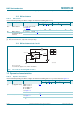
12.1 Waveforms and test circuits
t
dis
disable time S or OE to D+ or D;
see Figure 11
[5]
V
CC
= 3.0 V to 3.6 V - 3.9 25 - 30 ns
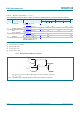
t
b-m
break-before-make
time
see Figure 12
[3]
V
CC
= 3.0 V to 3.6 V 2.0 5.9 - 2.0 - ns
t
sk(p)
pulse skew time see Figure 10
V
CC
= 3.0 V to 3.6 V
[3]
-20- - - ps
t
jit
jitter time R
L
=50; C
L
= 5 pF; t
r
, t
f
= 500 ps (10 % to 90 %) at
480 Mbs (PRBS = 2
15
1)
[3]
-200- - - ps
Table 9. Dynamic characteristics
…continued
At recommended operating conditions; voltages are referenced to GND (ground = 0 V); for test circuit see Figure 13.
Symbol Parameter Conditions T
amb
= 40 C to +85 C T
amb
= 40 C to +125 C Unit
Min Typ
[1]
Max Min Max
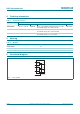
Logic levels: V
OL
and V
OH
are typical output voltage levels that occur with the output load.
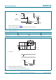
t
sk(p)
= |t
PHL
t
PLH
|.
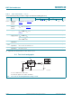
Fig 10. The data input to output propagation delay times and pulse skew time
aaa-001359
t
PHL
t
PLH
50%
50%
input
400 mV
GND
V
OH
V
OL
output