
Datasheet

NX3DV42 All information provided in this document is subject to legal disclaimers. © NXP B.V. 2013. All rights reserved.
Product data sheet Rev. 3 — 13 February 2013 7 of 19
NXP Semiconductors
NX3DV42
Dual high-speed USB 2.0 double-pole double-throw analog switch
11.2 ON resistance
[1] Typical values are measured at T
amb
= 25 C.
[2] Measured at identical V
CC
, temperature and input voltage.
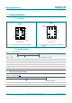
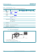
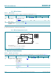
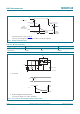
11.3 ON resistance test circuit
12. Dynamic characteristics
Table 8. ON resistance
At recommended operating conditions; voltages are referenced to GND (ground = 0 V).
Symbol Parameter Conditions T
amb
= 40 C to +85 C T
amb
= 40 C to +125 C Unit
Min Typ
[1]
Max Min Max
R
ON
ON resistance V
I
=0.4 V; I
SW
=8mA;
see Figure 9
V
CC
= 3.0 V - 3.9 6.5 - 10
R
ON
ON resistance
mismatch between
channels
V
I
= 0.4 V; I
SW
= 8 mA
[2]
V
CC
= 3.0 V - 0.65 - - -
R
ON
=V
SW
/ I
SW
.
Test circuit also applies for D+, HSD1+ and HSD2+.
Fig 9. Test circuit for measuring ON resistance
aaa-001366
2
1
HSD2-
V
IL
or V
IH
V
IL
HSD1-
S
D- switch
V
I
I
SW
GND
OE
V
CC
V
IL
V
IH
1
2
Sswitch
V
V
SW
Table 9. Dynamic characteristics
At recommended operating conditions; voltages are referenced to GND (ground = 0 V); for test circuit see Figure 13.
Symbol Parameter Conditions T
amb
= 40 C to +85 C T
amb
= 40 C to +125 C Unit
Min Typ
[1]
Max Min Max
t
pd
propagation delay HSDn+ to D+ or
HSDn to Dor
D+ to HSDn+ or
D to HSDn;
see Figure 10
[2][3]
V
CC
=3.3V - 0.25 - - - ns
t
en
enable time S or OE to D+ or D;
see Figure 11
[4]
V
CC
= 3.0 V to 3.6 V - 11.2 30 - 40 ns