
Datasheet

NX3DV42 All information provided in this document is subject to legal disclaimers. © NXP B.V. 2013. All rights reserved.
Product data sheet Rev. 3 — 13 February 2013 4 of 19
NXP Semiconductors
NX3DV42
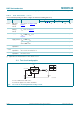
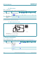
Dual high-speed USB 2.0 double-pole double-throw analog switch
9. Limiting values
[1] The minimum input voltage rating may be exceeded if the input current rating is observed.
[2] For XQFN10 packages: above 100 C derate linearly with 4 mW/K.
10. Recommended operating conditions
[1] To avoid sinking GND current from terminals D+ and D when switch current flows in terminals HSDn+ and HSDn, the voltage drop
across the bidirectional switch must not exceed 0.4 V. If the switch current flows into terminals D+ and D, no GND current will flow from
terminals HSDn+ and HSDn. In this case, there is no limit for the voltage drop across the switch.
11. Static characteristics
Table 5. Limiting values
In accordance with the Absolute Maximum Rating System (IEC 60134). Voltages are referenced to GND (ground = 0 V).
Symbol Parameter Conditions Min Max Unit
V
CC
supply voltage 0.5 +5.5 V
V
I
input voltage pins S and OE
[1]
0.5 +5.5 V
V
SW
switch voltage 0.5 +5.5 V
I
IK
input clamping current V
I
< 0.5 V 50 - mA
I
SK
switch clamping current V
I
< 0.5 V 50 - mA
I
SW
switch current - 100 mA
I
CC
supply current - +50 mA
T
stg
storage temperature 65 +150 C
P
tot
total power dissipation T
amb
= 40 Cto+125C
[2]
-250mW
Table 6. Recommended operating conditions
Symbol Parameter Conditions Min Max Unit
V
CC
supply voltage 3.0 4.3 V
V
I
input voltage pins S and OE 04.5V
V
SW
switch voltage
[1]
0V
CC
V
T
amb
ambient temperature 40 +125 C
Table 7. Static characteristics
At recommended operating conditions; voltages are referenced to GND (ground 0 V).
Symbol Parameter Conditions T
amb
= 40 C to +85 C T
amb
= 40 C to +125 C Unit
Min Typ
[1]
Max Min Max
V
IH
HIGH-level
input voltage
V
CC
= 3.0 V to 3.6 V 1.3 - - 1.3 - V
V
CC
=4.3V 1.7 - - 1.7 - V
V
IL
LOW-level
input voltage
V
CC
= 3.0 V to 3.6 V - - 0.5 - 0.5 V
V
CC
= 4.3 V - - 0.7 - 0.7 V
V
IK
input clamping
voltage
V
CC
=3.0V; I
I
= 18 mA - - 1.2 - 1.2 V
I
I
input leakage
current
pins S and OE;
V
I
= GND to 4.3 V; V
CC
=4.3V;
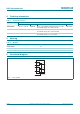
see Figure 5
--1- 10 A