
Datasheet

NX3DV42 All information provided in this document is subject to legal disclaimers. © NXP B.V. 2013. All rights reserved.
Product data sheet Rev. 3 — 13 February 2013 3 of 19
NXP Semiconductors
NX3DV42
Dual high-speed USB 2.0 double-pole double-throw analog switch
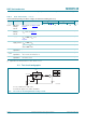
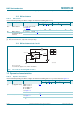
7. Pinning information
7.1 Pinning
7.2 Pin description
8. Functional description
[1] H = HIGH voltage level; L = LOW voltage level; X = don’t care.
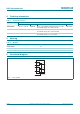
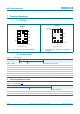
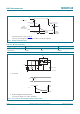
Fig 2. Pin configuration SOT1049-3 (XQFN10) Fig 3. Pin configuration SOT1160-1 and SOT1337-1
(XQFN10)
DDD
1;'9
7UDQVSDUHQWWRSYLHZ
2(
+6'
+6'
+6'
'
'
6
*1'
+6' 9
&&
NX3DV42
5HSD1+
GND
4HSD1-
3
OE8
10
V
CC
9
S
7 HSD2+
6 HSD2-
D+ 1
D- 2
terminal 1
index area
aaa-001357
Transparent top view
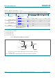
Table 3. Pin description
Symbol Pin Description
SOT1049-3 SOT1160-1, SOT1337-1
HSD1, HSD2 5, 7 4, 6 independent input or output
HSD1+, HSD2+ 6, 8 5, 7 independent input or output
D+, D 2, 3 1, 2 common output or input
GND 4 3 ground (0 V)
OE
9 8 output enable input (active LOW)
S 1 10 select input
V
CC
10 9 supply voltage
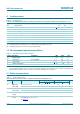
Table 4. Function table
[1]
Input Channel on
S OE
L L HSD1+ and HSD1
H L HSD2+ and HSD2
X H switch off