
Datasheet

NX3DV42 All information provided in this document is subject to legal disclaimers. © NXP B.V. 2013. All rights reserved.
Product data sheet Rev. 3 — 13 February 2013 11 of 19
NXP Semiconductors
NX3DV42
Dual high-speed USB 2.0 double-pole double-throw analog switch
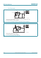
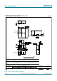
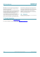
12.3 Test circuits
Adjust f
i
voltage to obtain 0 dBm level at output. Increase f
i
frequency until dB meter reads 3dB.
Test circuit also applies for D+, HSD1+ and HSD2+.
Fig 14. Test circuit for measuring the frequency response when channel is in ON-state
dB
aaa-001360
2
1
HSD2-
V
IL
or V
IH
V
IL
HSD1-
S
0.5V
CC
D-
switch
f
i
C
L
R
L
GND
OE
V
CC
V
IL
V
IH
1
2
Sswitch
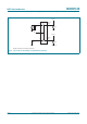
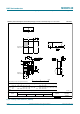
Adjust f
i
voltage to obtain 0 dBm level at input.
Test circuit also applies for D+, HSD1+ and HSD2+.
Fig 15. Test circuit for measuring isolation (OFF-state)
aaa-001367
2
1
HSD2-
V
IL
or V
IH
V
IH
HSD1-
S
D- switch
f
i
R
L
R
L
GND
OE
V
CC
0.5V
CC
V
IH
V
IL
1
2
Sswitch
dB
0.5V
CC