
Datasheet


MPC8309 PowerQUICC II Pro Integrated Communications Processor Family Hardware Specifications, Rev. 2
Freescale Semiconductor 9
Electrical characteristics
2.1.2 Power supply voltage specification
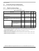
The following table provides the recommended operating conditions for the MPC8309. Note that these
values are the recommended and tested operating conditions. Proper device operation outside of these
conditions is not guaranteed.
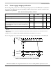
The following figure shows the undershoot and overshoot voltages at the interfaces of the MPC8309
Figure 2. Overshoot/Undershoot voltage for GV
DD
/OV
DD
Table 2. Recommended operating conditions
Characteristic Symbol
Recommended
Value
Unit Note
Core supply voltage V
DD
1.0V±50mV V 1
PLL supply voltage AV
DD1
AV
DD2
AV
DD3
1.0V±50mV V 1
DDR2 DRAM I/O voltage GV
DD
1.8 V ± 100 mV V 1
PCI, Local bus, DUART, system control and power management,
I
2
C, SPI, MII, RMII, MII management, eSDHC, FlexCAN,USB and
JTAG I/O voltage
OV
DD
3.3 V ± 300 mV V 1, 3
Junction temperature T
A
/T
J
0to105 °C2
Notes:
1. GV
DD
, OV
DD
, AV
DD
, and V
DD
must track each other and must vary in the same direction—either in the positive or negative
direction.
2. Minimum temperature is specified with T
A
(Ambient Temperature); maximum temperature is specified with T
J
(Junction
Temperature).
3. OVDD here refers to NVDDA, NVDDB, NVDDC, NVDDF, NVDDG, and NVDDH from the ball map.
GND
GND – 0.3 V
GND – 0.7 V
Not to Exceed 10%
G/OV
DD
+ 20%
G/OV
DD
G/OV
DD
+ 5%
of t
interface
1
1. t
interface
refers to the clock period associated with the bus clock interface.
V
IH
V
IL
Note: