
Datasheet


MPC8309 PowerQUICC II Pro Integrated Communications Processor Family Hardware Specifications, Rev. 2
8 Freescale Semiconductor
Electrical characteristics
2.1 Overall DC electrical characteristics
This section covers the ratings, conditions, and other characteristics.
2.1.1 Absolute maximum ratings
The following table provides the absolute maximum ratings.
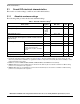
Table 1. Absolute maximum ratings
1
Characteristic Symbol Max Value Unit Notes
Core supply voltage V
DD
–0.3to1.26 V —
PLL supply voltage AV
DD1
AV
DD2
AV
DD3
–0.3to1.26 V —
DDR2 DRAM I/O voltage GV
DD
–0.3to1.98 V —
PCI, Local bus, DUART, system control and power management,
I
2
C, SPI, MII, RMII, MII management, eSDHC, FlexCAN, USB and
JTAG I/O voltage
OV
DD
–0.3 to 3.6 V 2
Input voltage DDR2 DRAM signals MV
IN
–0.3to(GV
DD
+0.3) V 3
DDR2 DRAM reference MV
REF
–0.3to(GV
DD
+0.3) V 3
Local bus, DUART, SYS_CLK_IN,
system control and power
management, I
2
C, SPI, and JTAG
signals
OV
IN
–0.3 to (OV
DD
+0.3) V 4
PCI OV
IN
–0.3 to (OV
DD
+ 0.3) V
Storage temperature range T
STG
–55 to 150 °C—
Notes:
1. Functional and tested operating conditions are given in Ta bl e 2 . Absolute maximum ratings are stress ratings only, and
functional operation at the maximums is not guaranteed. Stresses beyond those listed may affect device reliability or cause
permanent damage to the device.
2. OVDD here refers to NVDDA, NVDDB, NVDDC, NVDDF, NVDDG, and NVDDH from the ball map.
3. Caution: MV
IN
must not exceed GV
DD
by more than 0.3 V. This limit may be exceeded for a maximum of 100 ms during
power-on reset and power-down sequences.
4. Caution: OV
IN
must not exceed OV
DD
by more than 0.3 V. This limit may be exceeded for a maximum of 100 ms during
power-on reset and power-down sequences.