
Datasheet


MPC8309 PowerQUICC II Pro Integrated Communications Processor Family Hardware Specifications, Rev. 2
66 Freescale Semiconductor
Clocking
23.4 System PLL configuration
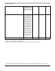
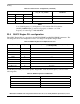
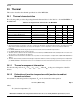
The system PLL is controlled by the RCWL[SPMF] parameter. Table 56 shows the multiplication factor
encodings for the system PLL.
NOTE
System PLL VCO frequency = 2 × (CSB frequency) × (System PLL VCO
divider). The VCO divider needs to be set properly so that the System PLL
VCO frequency is in the range of 450–750 MHz.
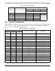
As described in Section 23, “Clocking,” the LBCM, DDRCM, and SPMF parameters in the reset
configuration word low select the ratio between the primary clock input (SYS_CLK_IN) and the internal
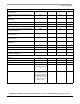
coherent system bus clock (csb_clk). The following table shows the expected frequency values for the CSB
frequency for selected csb_clk to SYS_CLK_IN ratios.
DDR2 memory bus frequency (MCLK)
2
167 MHz
Local bus frequency (LCLK
n
)
3
66 MHz
Notes:
1. The SYS_CLK_IN frequency, RCWL[SPMF], and RCWL[COREPLL] settings must be chosen such that the resulting
csb_clk, MCLK, LCLK, and core_clk frequencies do not exceed their respective maximum or minimum operating
frequencies.
2. The DDR2 data rate is 2× the DDR2 memory bus frequency.
3. The local bus frequency is 1/2, 1/4, or 1/8 of the lb_clk frequency (depending on LCRR[CLKDIV]) which is in turn 1× or 2×
the csb_clk frequency (depending on RCWL[LBCM]).
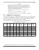
Table 56. System PLL multiplication factors
RCWL[SPMF] System PLL Multiplication Factor
0000 Reserved
0001 Reserved
0010 × 2
0011 × 3
0100 × 4
0101 × 5
0110 × 6
0111–1111 Reserved
Table 55. Operating Frequencies for MAPBGA (continued)
Characteristic
1
Max Operating Frequency Unit