
Datasheet


MPC8309 PowerQUICC II Pro Integrated Communications Processor Family Hardware Specifications, Rev. 2
Freescale Semiconductor 65
Clocking
Configuration chapter in the MPC8309 PowerQUICC II Pro Integrated Communications Processor
Family Reference Manual.
The qe_clk frequency is determined by the QUICC Engine PLL multiplication factor (RCWL[CEPMF])
and the QUICC Engine PLL division factor (RCWL[CEPDF]) as the following equation:
qe_clk = (QE_CLK_IN × CEPMF) ÷ (1 + CEPDF) Eqn. 3
For more information, see the QUICC Engine PLL Multiplication Factor section and the “QUICC Engine
PLL Division Factor” section in the MPC8309 PowerQUICC II Pro Integrated Communications
Processor Family Reference Manual for more information.
The DDR SDRAM memory controller operates with a frequency equal to twice the frequency of csb_clk.
Note that ddr_clk is not the external memory bus frequency; ddr_clk passes through the DDR clock divider
(÷2) to create the differential DDR memory bus clock outputs (MCK and MCK). However, the data rate
is the same frequency as ddr_clk.
The local bus memory controller operates with a frequency equal to the frequency of csb_clk. Note that
lbc_clk is not the external local bus frequency; lbc_clk passes through the LBC clock divider to create the
external local bus clock outputs (LCLK). The LBC clock divider ratio is controlled by LCRR[CLKDIV].
For more information, see the LBC Bus Clock and Clock Ratios section in the MPC8309 PowerQUICC
II Pro Integrated Communications Processor Family Reference Manual.
In addition, some of the internal units may be required to be shut off or operate at lower frequency than
the csb_clk frequency. These units have a default clock ratio that can be configured by a memory mapped
register after the device comes out of reset.
The following table specifies which units have a configurable clock frequency. For detailed description,
refer to the “System Clock Control Register (SCCR)” section in the MPC8309 PowerQUICC II Pro
Integrated Communications Processor Family Reference Manual.
NOTE
Setting the clock ratio of these units must be performed prior to any access
to them.
The following table provides the maximum operating frequencies for the MPC8309 MAPBGA under
recommended operating conditions (see Table 2).
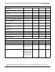
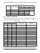
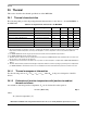
Table 54. Configurable clock units
Unit Default Frequency Options
I2C,SDHC, USB, DMA Complex
csb_clk
Off, csb_clk,
csb_clk
/2,
csb_clk
/3
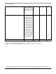
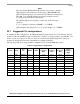
Table 55. Operating Frequencies for MAPBGA
Characteristic
1
Max Operating Frequency Unit
e300 core frequency (
core_clk
)417MHz
Coherent system bus frequency (
csb_clk
)167MHz
QUICC Engine frequency (
qe_clk
)233MHz