
Datasheet
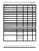
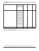


MPC8309 PowerQUICC II Pro Integrated Communications Processor Family Hardware Specifications, Rev. 2
Freescale Semiconductor 63
Clocking
23 Clocking
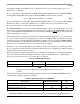
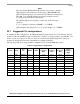
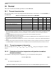
The following figure shows the internal distribution of clocks within the MPC8309.
Figure 43. MPC8309 clock subsystem
The primary clock source for the MPC8309 can be one of three inputs,Crystal(SYS_XTAL_IN ),
SYS_CLK_IN or PCI_SYNC_IN, depending on whether the device is configured in PCI host or PCI agent
mode, respectively.
Core PLL
System
LBC
LCLK[0:1]
core_clk
e300c3 core
csb_clk
Local Bus
Clock
Unit
of the device
lbc_clk
Memory
Device
/n
Clock
MEMC_MCK
MEMC_MCK
DDR
ddr_clk
DDR
Memory
Device
PLL
to DDR
memory
controller
Clock
/2
Divider
Divider
QE PLL
CLK Gen
QE Block
qe_clk
QE_CLK_IN
PCI Clock Divider
csb_clk
to rest
to local bus
CFG_CLKIN_DIV
PCI_SYNC_OUT
PCI_CLK[0:2]
PCI_SYNC_IN
/n
MPC8309
Rest of the System
SYS_XTAL_OUT
SYS_XTAL_IN
SYS_CLK_IN
CRYSTAL