
Datasheet


MPC8309 PowerQUICC II Pro Integrated Communications Processor Family Hardware Specifications, Rev. 2
62 Freescale Semiconductor
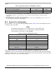
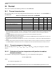
Package and pin listings
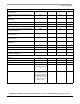
VDD H8,H9,H10,H11,H12,M8,
H13,N16,H14,H15,H16,
P16,P8,L8,K16,J16,K8,J
8,R8,T16,R16,T8,T9,T11
,T10,T12,T13,T14,T15
---
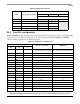
VSS A1, C3, F22, J14, K14,
M15, L15, N20, R9, Y21,
T20, AB21, B1, C22,G4,
K15, J15, M2, M22, P9,
R10, V2, AA2, AC1,
B4,D5, G20, J22, K20,
M5, N9, P10, R11, V22,
AA22,AC23, B6, D8, J2,
K4, M9,L9, N10, P11,
R12, W4, AB4, D11, B9,
J9, K9, L10,M10, N11,
P12, R13, Y7,AB6, B12,
D14, J10, K10, L11, M11,
P13, N12, R14,
Y10,AB9, B15, D17, J11,
K11, D20, B18, J12, K12,
L13, L12, L14, K13, J13,
F2, B21, M14, M13, M12,
Y19, Y16, AB15, AB12,
Y13, N13, N14, N15,
P14, P15, R2, AB18,
R15, R21, T4
---
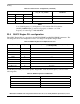
NC A23 - - -
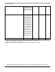
Notes
1. This pin is an open drain signal. A weak pull-up resistor should be placed on this pin to OV
DD
2 This pin has weak pull-up that is always enabled.
4. OVDD here refers to NVDDA, NVDDB,NVDDC, NVDDF, NVDDG, and NVDDH from the ball map.