
Datasheet

MPC8309 PowerQUICC II Pro Integrated Communications Processor Family Hardware Specifications, Rev. 2
Freescale Semiconductor 49
JTAG
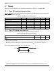
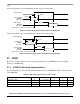
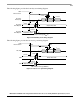
The following figure provides the boundary-scan timing diagram.
Figure 40. Boundary-Scan timing diagram
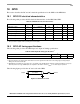
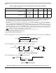
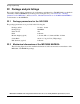
The following figure provides the test access port timing diagram.
Figure 41. Test access port timing diagram
VM = Midpoint Voltage (OV
DD
/2)
VM VM
t
JTDVKH
t
JTDXKH
Boundary
Data Outputs
Boundary
Data Outputs
JTAG
External Clock
Boundary
Data Inputs
Output Data Valid
t
JTKLDX
t
JTKLDZ
t
JTKLDV
Input
Data Valid
Output Data Valid
VM = Midpoint Voltage (OV
DD
/2)
VM VM
t
JTIVKH
t
JTIXKH
JTAG
External Clock
Output Data Valid
t
JTKLOX
t
JTKLOZ
t
JTKLOV
Input
Data Valid
Output Data Valid
TDI, TMS
TDO
TDO