
Datasheet

MPC8309 PowerQUICC II Pro Integrated Communications Processor Family Hardware Specifications, Rev. 2
48 Freescale Semiconductor
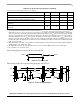
JTAG
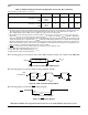
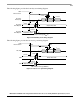
The following figure provides the AC test load for TDO and the boundary-scan outputs of the MPC8309.
Figure 37. AC test load for the JTAG interface
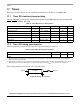
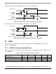
The following figure provides the JTAG clock input timing diagram.
Figure 38. JTAG clock input timing diagram
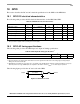
The following figure provides the TRST timing diagram.
Figure 39. TRST timing diagram
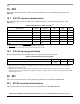
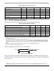
Output hold times:
Boundary-scan data
TDO
t
JTKLDX
t
JTKLOX
2
2
—
—
ns
5
JTAG external clock to output high impedance:
Boundary-scan data
TDO
t
JTKLDZ
t
JTKLOZ
2
2
19
9
ns
5, 6
6
Notes:
1. All outputs are measured from the midpoint voltage of the falling/rising edge of t
TCLK
to the midpoint of the signal in question.
The output timings are measured at the pins. All output timings assume a purely resistive 50-Ω load (see Figure 37).
Time-of-flight delays must be added for trace lengths, vias, and connectors in the system.
2. The symbols used for timing specifications follow the pattern of t
(first two letters of functional block)(signal)(state)(reference)(state)
for
inputs and t
(first two letters of functional block)(reference)(state)(signal)(state)
for outputs. For example, t
JTDVKH
symbolizes JTAG device
timing (JT) with respect to the time data input signals (D) reaching the valid state (V) relative to the t
JTG
clock reference (K)
going to the high (H) state or setup time. Also, t
JTDXKH
symbolizes JTAG timing (JT) with respect to the time data input signals
(D) went invalid (X) relative to the t
JTG
clock reference (K) going to the high (H) state. Note that, in general, the clock reference
symbol representation is based on three letters representing the clock of a particular functional. For rise and fall times, the
latter convention is used with the appropriate letter: R (rise) or F (fall).
3. TRST
is an asynchronous level sensitive signal. The setup time is for test purposes only.
4. Non-JTAG signal input timing with respect to t
TCLK
.
5. Non-JTAG signal output timing with respect to t
TCLK
.
6. Guaranteed by design and characterization.
Table 52. JTAG AC timing specifications (independent of SYS_CLK_IN)
1
(continued)
At recommended operating conditions (see Ta ble 2 ).
Parameter Symbol
2
Min Max Unit Notes
Output
Z
0
= 50 Ω
OV
DD
/2
R
L
= 50 Ω
JTAG
t
JTKHKL
t
JTGR
External Clock
VMVMVM
t
JTG
t
JTGF
VM = Midpoint Voltage (OV
DD
/2)
TRST
VM = Midpoint Voltage (OV
DD
/2)
VM VM
t
TRST