
Datasheet

MPC8309 PowerQUICC II Pro Integrated Communications Processor Family Hardware Specifications, Rev. 2
Freescale Semiconductor 47
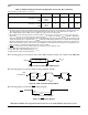
JTAG
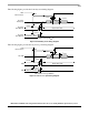
21.2 JTAG AC electrical characteristics
This section describes the AC electrical specifications for the IEEE Std. 1149.1 (JTAG) interface of the
MPC8309. The following table provides the JTAG AC timing specifications as defined in Figure 38
through Figure 41.
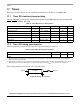
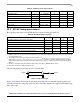
Input high voltage V
IH
—2.0OV
DD
+0.3 V
Input low voltage V
IL
— –0.3 0.8 V
Input current I
IN
0 V ≤ V
IN
≤ OV
DD
—±5 μA
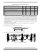
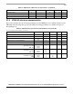
Table 52. JTAG AC timing specifications (independent of SYS_CLK_IN)
1
At recommended operating conditions (see Ta ble 2 ).
Parameter Symbol
2
Min Max Unit Notes
JTAG external clock frequency of operation f
JTG
0 33.3 MHz —
JTAG external clock cycle time t
JTG
30 — ns —
JTAG external clock pulse width measured at 1.4 V t
JTKHKL
11 — ns —
JTAG external clock rise and fall times t
JTGR
, t
JTGF
02ns—
TRST
assert time t
TRST
25 — ns 3
Input setup times:
Boundary-scan data
TMS, TDI
t
JTDVKH
t
JTIVKH
4
4
—
—
ns
4
Input hold times:
Boundary-scan data
TMS, TDI
t
JTDXKH
t
JTIXKH
10
10
—
—
ns
4
Valid t imes:
Boundary-scan data
TDO
t
JTKLDV
t
JTKLOV
2
2
15
15
ns
5
Table 51. JTAG interface DC electrical characteristics (continued)
Characteristic Symbol Condition Min Max Unit