
Datasheet

MPC8309 PowerQUICC II Pro Integrated Communications Processor Family Hardware Specifications, Rev. 2
46 Freescale Semiconductor
JTAG
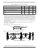
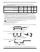
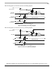
The following figure shows the SPI timing in slave mode (external clock).
Figure 35. SPI AC Timing in slave mode (external clock) diagram
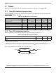
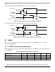
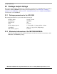
The following figure shows the SPI timing in master mode (internal clock).
Figure 36. SPI AC timing in master mode (internal clock) diagram
21 JTAG
This section describes the DC and AC electrical specifications for the IEEE Std. 1149.1™ (JTAG)
interface of the MPC8309.
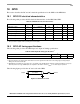
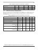
21.1 JTAG DC electrical characteristics
The following table provides the DC electrical characteristics for the IEEE Std. 1149.1 (JTAG) interface
of the MPC8309.
Table 51. JTAG interface DC electrical characteristics
Characteristic Symbol Condition Min Max Unit
Output high voltage V
OH
I
OH
= –6.0 mA 2. 4 — V
Output low voltage V
OL
I
OL
= 6.0 mA — 0.5 V
Output low voltage V
OL
I
OL
= 3.2 mA — 0.4 V
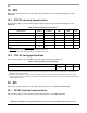
SPICLK (Input)
t
NEIXKH
t
NEIVKH
t
NEKHOV
Input Signals:
SPIMOSI
(See Note)
Output Signals:
SPIMISO
(See Note)
Note: The clock edge is selectable on SPI.
SPICLK (Output)
t
NIIXKH
t
NIKHOV
Input Signals:
SPIMISO
(See Note)
Output Signals:
SPIMOSI
(See Note)
Note: The clock edge is selectable on SPI.
t
NIIVKH