
Datasheet


MPC8309 PowerQUICC II Pro Integrated Communications Processor Family Hardware Specifications, Rev. 2
40 Freescale Semiconductor
I
2
C
16 I
2
C
This section describes the DC and AC electrical characteristics for the I
2
C interface of the MPC8309.
16.1 I
2
C DC electrical characteristics
The following table provides the DC electrical characteristics for the I
2
C interface of the MPC8309.
16.2 I
2
C AC electrical specifications
The following table provides the AC timing parameters for the I
2
C interface of the MPC8309.
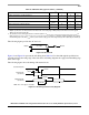
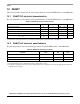
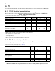
Table 41. I
2
C DC electrical characteristics
At recommended operating conditions with OV
DD
of 3.3 V ± 300mV.
Parameter Symbol Min Max Unit Notes
Input high voltage level V
IH
0.7 × OV
DD
OV
DD
+0.3 V —
Input low voltage level V
IL
–0.3 0.3 × OV
DD
V—
Low level output voltage V
OL
00.4V1
Output fall time from V
IH
(min) to V
IL
(max) with a bus
capacitance from 10 to 400 pF
t
I2KLKV
20 + 0.1 × C
B
250 ns 2
Pulse width of spikes which must be suppressed by the
input filter
t
I2KHKL
050ns3
Capacitance for each I/O pin C
I
—10pF—
Input current (0 V ≤ V
IN
≤ OV
DD
)I
IN
—±5 μA4
Notes:
1. Output voltage (open drain or open collector) condition = 3 mA sink current.
2. C
B
= capacitance of one bus line in pF.
3. Refer to the
MPC
8309
PowerQUICC II Pro Integrated Communications Processor Family Reference Manual
for information
on the digital filter used.
4. I/O pins obstructs the SDA and SCL lines if OV
DD
is switched off.
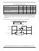
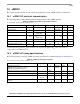
Table 42. I
2
C AC electrical specifications
All values refer to V
IH
(min) and V
IL
(max) levels (see Ta b le 41 ).
Parameter Symbol
1
Min Max Unit
SCL clock frequency f
I2C
0400kHz
Low period of the SCL clock t
I2CL
1.3 — μs
High period of the SCL clock t
I2CH
0.6 — μs
Setup time for a repeated START condition t
I2SVKH
0.6 — μs
Hold time (repeated) START condition (after this period, the first clock
pulse is generated)
t
I2SXKL
0.6 — μs
Data setup time t
I2DVKH
100 — ns
Data hold time: I
2
C bus devices t
I2DXKL
300 0.9
3
μs
Rise time of both SDA and SCL signals t
I2CR
20 + 0.1 C
B
4
300 ns