
Datasheet


MPC8309 PowerQUICC II Pro Integrated Communications Processor Family Hardware Specifications, Rev. 2
Freescale Semiconductor 35
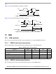
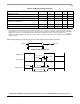
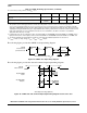
USB
The following figures provide the AC test load and signals for the USB, respectively.
Figure 26. USB AC test load
Figure 27. USB signals
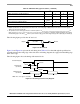
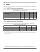
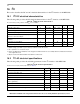
Table 34. USB general timing parameters
Parameter Symbol
1
Min Max Unit Note
USB clock cycle time t
USCK
15 — ns —
Input setup to USB clock—all inputs t
USIVKH
4—ns—
input hold to USB clock—all inputs t
USIXKH
1—ns—
USB clock to output valid—all outputs (except
USBDR_STP_USBDR_STP)
t
USKHOV
—7ns—
USB clock to output valid—USBDR_STP t
USKHOV
—7.5ns—
Output hold from USB clock—all outputs t
USKHOX
2—ns—
Note:
1. The symbols used for timing specifications follow the pattern of t
(first two letters of functional block)(signal)(state)(reference)(state)
for
inputs and t
(first two letters of functional block)(reference)(state)(signal)(state)
for outputs. For example, t
USIXKH
symbolizes USB timing
(USB) for the input (I) to go invalid (X) with respect to the time the USB clock reference (K) goes high (H). Also, t
USKHOX
symbolizes us timing (USB) for the USB clock reference (K) to go high (H), with respect to the output (O) going invalid (X) or
output hold time.
Output
Z
0
= 50 Ω
OV
DD
/2
R
L
= 50 Ω
Output Signals
t
USKHOV
USBDR_CLK
Input Signals
t
USIXKH
t
USIVKH
t
USKHOX