
Datasheet


MPC8309 PowerQUICC II Pro Integrated Communications Processor Family Hardware Specifications, Rev. 2
32 Freescale Semiconductor
PCI
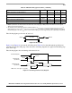
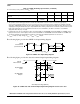
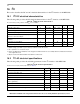
The following figure shows the timing with internal clock.
Figure 22. AC timing (internal clock) diagram
11 PCI
This section describes the DC and AC electrical specifications for the PCI bus of the MPC8309.
11.1 PCI DC electrical characteristics
Table 30 provides the DC electrical characteristics for the PCI interface of the MPC8309.
11.2 PCI AC electrical specifications
This section describes the general AC timing parameters of the PCI bus of the MPC8309. Note that the
PCI_CLK or PCI_SYNC_IN signal is used as the PCI input clock depending on whether the MPC8309 is
configured as a host or agent device. Table 31 shows the PCI AC timing specifications at 66 MHz.
.
Table 32 shows the PCI AC timing specifications at 33 MHz.
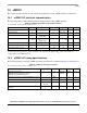
Table 30. PCI DC electrical characteristics
1,2
Parameter Symbol Test Condition Min Max Unit
High-level input voltage V
IH
V
OUT
≥ V
OH
(min) or 2 OV
DD
+ 0.3 V
Low-level input voltage V
IL
V
OUT
≤ V
OL
(max) –0.3 0.8 V
High-level output voltage V
OH
OV
DD
= min,
I
OH
= –100 μA
OV
DD
– 0.2 — V
Low-level output voltage V
OL
OV
DD
= min,
I
OL
= 100 μA
—0.2V
Input current I
IN
0 V ≤ V
IN
≤ OV
DD
— ± 5 μA
Notes:
1. Note that the symbol V
IN
, in this case, represents the OV
IN
symbol referenced in Ta bl e 1 and Tab le 2 .
2. Ranges listed do not meet the full range of the DC specifications of the
PCI 2.3 Local Bus Specifications.
Serial CLK (Output)
t
HIIXKH
t
HIKHOV
Input Signals:
(See Note)
Output Signals:
(See Note)
t
HIIVKH
t
HIKHOX
Note: The clock edge is selectable.