
Datasheet


MPC8309 PowerQUICC II Pro Integrated Communications Processor Family Hardware Specifications, Rev. 2
Freescale Semiconductor 31
HDLC
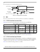
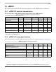
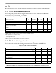
The following figure provides the AC test load.
Figure 20. AC test load
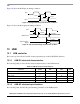
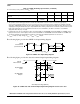
Figure 21 and Figure 22 represent the AC timing from Table 29. Note that although the specifications
generally reference the rising edge of the clock, these AC timing diagrams also apply when the falling edge
is the active edge.
The following figure shows the timing with external clock.
Figure 21. AC timing (external clock) diagram
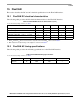
Outputs—External clock high impedance t
HEKHOX
18ns
Inputs—Internal clock input setup time t
HIIVKH
9—ns
Inputs—External clock input setup time t
HEIVKH
4—ns
Inputs—Internal clock input hold time t
HIIXKH
0—ns
Inputs—External clock input hold time t
HEIXKH
1—ns
Notes:
1. Output specifications are measured from the 50% level of the rising edge of QE_CLK_IN to the 50% level of the signal.
Timings are measured at the pin.
2. The symbols used for timing specifications follow the pattern of t
(first two letters of functional block)(signal)(state)(reference)(state)
for
inputs and t
(first two letters of functional block)(reference)(state)(signal)(state)
for outputs. For example, t
HIKHOX
symbolizes the outputs
internal timing (HI) for the time t
serial
memory clock reference (K) goes from the high state (H) until outputs (O) are invalid (X).
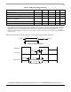
Table 29. HDLC AC timing specifications
1
(continued)
Characteristic Symbol
2
Min Max Unit
Output
Z
0
= 50 Ω
OV
DD
/2
R
L
= 50 Ω
Serial CLK (Input)
t
HEIXKH
t
HEIVKH
t
HEKHOV
Input Signals:
(See Note)
Output Signals:
(See Note)
Note: The clock edge is selectable.
t
HEKHOX