
Datasheet

MPC8309 PowerQUICC II Pro Integrated Communications Processor Family Hardware Specifications, Rev. 2
30 Freescale Semiconductor
HDLC
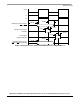
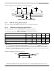
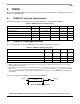
The following figure represents the AC timing from Table 27. Note that although the specifications
generally reference the rising edge of the clock, these AC timing diagrams also apply when the falling edge
is the active edge.
Figure 19. TDM/SI AC timing (external clock) diagram
10 HDLC
This section describes the DC and AC electrical specifications for the high level data link control (HDLC),
of the MPC8309.
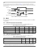
10.1 HDLC DC electrical characteristics
The following table provides the DC electrical characteristics for the MPC8309 HDLC protocol.
10.2 HDLC AC timing specifications
The following table provides the input and output AC timing specifications for HDLC protocol.
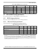
Table 28. HDLC DC electrical characteristics
Characteristic Symbol Condition Min Max Unit
Output high voltage V
OH
I
OH
= –2.0 mA 2.4 — V
Output low voltage V
OL
I
OL
= 3.2 mA — 0.5 V
Input high voltage V
IH
—2.0OV
DD
+0.3 V
Input low voltage V
IL
— –0.3 0.8 V
Input current I
IN
0 V ≤ V
IN
≤ OV
DD
— ± 5 μA
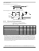
Table 29. HDLC AC timing specifications
1
Characteristic Symbol
2
Min Max Unit
Outputs—Internal clock delay t
HIKHOV
09ns
Outputs—External clock delay t
HEKHOV
1 12 ns
Outputs—Internal clock high impedance t
HIKHOX
05.5ns
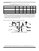
TDM/SICLK (Input)
t
SEIXKH
t
SEIVKH
t
SEKHOV
Input Signals:
TDM/SI
(See Note)
Output Signals:
TDM/SI
(See Note)
Note: The clock edge is selectable on TDM/SI.
t
SEKHOX