
Datasheet

MPC8309 PowerQUICC II Pro Integrated Communications Processor Family Hardware Specifications, Rev. 2
Freescale Semiconductor 29
TDM/SI
9TDM/SI
This section describes the DC and AC electrical specifications for the time-division-multiplexed and serial
interface of the MPC8309.
9.1 TDM/SI DC electrical characteristics
The following table provides the DC electrical characteristics for the MPC8309 TDM/SI.
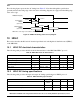
9.2 TDM/SI AC timing specifications
The following table provides the TDM/SI input and output AC timing specifications.
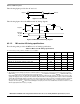
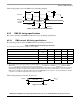
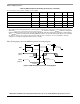
The following figure
provides the AC test load for the TDM/SI.
Figure 18. TDM/SI AC test load
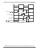
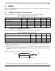
Table 26. TDM/SI DC electrical characteristics
Characteristic Symbol Condition Min Max Unit
Output high voltage V
OH
I
OH
= –2.0 mA 2.4 — V
Output low voltage V
OL
I
OL
= 3.2 mA — 0.5 V
Input high voltage V
IH
—2.0OV
DD
+0.3 V
Input low voltage V
IL
— –0.3 0.8 V
Input current I
IN
0 V ≤ V
IN
≤ OV
DD
—±5μA
Table 27. TDM/SI AC timing specifications
1
Characteristic Symbol
2
Min Max Unit
TDM/SI outputs—External clock delay t
SEKHOV
214ns
TDM/SI outputs—External clock High Impedance t
SEKHOX
210ns
TDM/SI inputs—External clock input setup time t
SEIVKH
5—ns
TDM/SI inputs—External clock input hold time t
SEIXKH
2—ns
Notes:
1. Output specifications are measured from the 50% level of the rising edge of QE_CLK_IN to the 50% level of the signal.
Timings are measured at the pin.
2. The symbols used for timing specifications follow the pattern of t
(first two letters of functional block)(signal)(state)(reference)(state)
for
inputs and t
(first two letters of functional block)(reference)(state)(signal)(state)
for outputs. For example, t
SEKHOX
symbolizes the TDM/SI
outputs external timing (SE) for the time t
TDM/SI
memory clock reference (K) goes from the high state (H) until outputs (O)
are invalid (X).
Output
Z
0
= 50 Ω
OV
DD
/2
R
L
= 50 Ω