
Datasheet

MPC8309 PowerQUICC II Pro Integrated Communications Processor Family Hardware Specifications, Rev. 2
28 Freescale Semiconductor
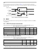
Ethernet and MII management
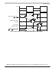
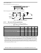
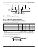
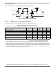
The following figure shows the MII management AC timing diagram.
Figure 17. MII management interface timing diagram
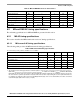
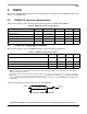
MDC to MDIO delay t
MDKHDX
10 — 70 ns —
MDIO to MDC setup time t
MDDVKH
8.5 — — ns —
MDIO to MDC hold time t
MDDXKH
0——ns—
MDC rise time t
MDCR
— — 10 ns —
MDC fall time t
MDHF
— — 10 ns —
Note:
1. The symbols used for timing specifications follow the pattern of t
(first two letters of functional block)(signal)(state)(reference)(state)
for
inputs and t
(first two letters of functional block)(reference)(state)(signal)(state)
for outputs. For example, t
MDKHDX
symbolizes management
data timing (MD) for the time t
MDC
from clock reference (K) high (H) until data outputs (D) are invalid (X) or data hold time.
Also, t
MDDVKH
symbolizes management data timing (MD) with respect to the time data input signals (D) reach the valid state
(V) relative to the t
MDC
clock reference (K) going to the high (H) state or setup time. For rise and fall times, the latter
convention is used with the appropriate letter: R (rise) or F (fall).
Table 25. MII management AC timing specifications (continued)
At recommended operating conditions with OV
DD
is 3.3 V ± 300mV.
Parameter/Condition Symbol
1
Min Typical Max Unit Note
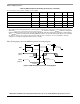
MDC
t
MDDXKH
t
MDC
t
MDCH
t
MDCR
t
MDCF
t
MDDVKH
t
MDKHDX
MDIO
MDIO
(Input)
(Output)