
Datasheet

MPC8309 PowerQUICC II Pro Integrated Communications Processor Family Hardware Specifications, Rev. 2
Freescale Semiconductor 27
Ethernet and MII management
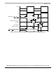
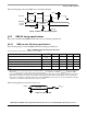
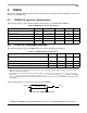
The following figure shows the RMII receive AC timing diagram.
Figure 16. RMII receive AC timing diagram
8.3 Ethernet management interface electrical characteristics
The electrical characteristics specified here apply to MII management interface signals MDIO
(management data input/output) and MDC (management data clock). The electrical characteristics for
MII, and RMII are specified in Section 8.1, “Ethernet controller (10/100 Mbps)—MII/RMII electrical
characteristics.”
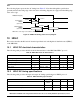
8.3.1 MII management DC electrical characteristics
MDC and MDIO are defined to operate at a supply voltage of 3.3 V. The DC electrical characteristics for
MDIO and MDC are provided in the following table.
8.3.2 MII management AC electrical specifications
The following table provides the MII management AC timing specifications.
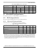
Table 24. MII management DC electrical characteristics when powered at 3.3 V
Parameter Symbol Conditions Min Max Unit
Supply voltage (3.3 V) OV
DD
—33.6V
Output high voltage V
OH
I
OH
= –1.0 mA OV
DD
=Min 2.40 OV
DD
+ 0.3 V
Output low voltage V
OL
I
OL
=1.0mA OV
DD
= Min GND 0. 50 V
Input high voltage V
IH
—2.00—V
Input low voltage V
IL
——0.80V
Input current I
IN
0 V ≤ V
IN
≤ OV
DD
—±5μA
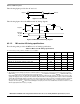
Table 25. MII management AC timing specifications
At recommended operating conditions with OV
DD
is 3.3 V ± 300mV.
Parameter/Condition Symbol
1
Min Typical Max Unit Note
MDC frequency f
MDC
—2.5—MHz—
MDC period t
MDC
—400—ns—
MDC clock pulse width high t
MDCH
32 — — ns —
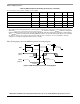
REF_CLK
RXD[1:0]
t
RMRDXKH
t
RMX
t
RMXH
t
RMXR
t
RMXF
CRS_DV
RX_ER
t
RMRDVKH
Valid D ata