
Datasheet

MPC8309 PowerQUICC II Pro Integrated Communications Processor Family Hardware Specifications, Rev. 2
Freescale Semiconductor 25
Ethernet and MII management
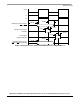
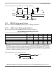
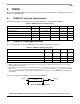
The following figure shows the MII receive AC timing diagram.
Figure 13. MII receive AC timing diagram
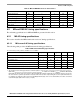
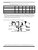
8.2.2 RMII AC timing specifications
This section describes the RMII transmit and receive AC timing specifications.
8.2.2.1 RMII transmit AC timing specifications
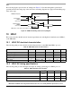
The following table provides the RMII transmit AC timing specifications.
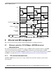
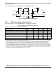
The following figure
provides the AC test load.
Figure 14. AC test load
Table 22. RMII transmit AC timing specifications
At recommended operating conditions with OV
DD
of 3.3 V ± 300mV.
Parameter/Condition Symbol
1
Min Typical Max Unit
REF_CLK clock t
RMX
—20—ns
REF_CLK duty cycle t
RMXH
/t
RMX
35 — 65 %
REF_CLK to RMII data TXD[1:0], TX_EN delay t
RMTKHDX
2 — 13 ns
REF_CLK data clock rise V
IL
(min) to V
IH
(max) t
RMXR
1.0 — 4.0 ns
REF_CLK data clock fall V
IH
(max) to V
IL
(min) t
RMXF
1.0 — 4.0 ns
Note:
1. The symbols used for timing specifications follow the pattern of t
(first three letters of functional block)(signal)(state)(reference)(state)
for
inputs and t
(first two letters of functional block)(reference)(state)(signal)(state)
for outputs. For example, t
RMTKHDX
symbolizes RMII
transmit timing (RMT) for the time t
RMX
clock reference (K) going high (H) until data outputs (D) are invalid (X). Note that, in
general, the clock reference symbol representation is based on two to three letters representing the clock of a particular
functional. For example, the subscript of t
RMX
represents the RMII(RM) reference (X) clock. For rise and fall times, the latter
convention is used with the appropriate letter: R (rise) or F (fall).
RX_CLK
RXD[3:0]
t
MRDXKH
t
MRX
t
MRXH
t
MRXR
t
MRXF
RX_DV
RX_ER
t
MRDVKH
Valid D ata
Output
Z
0
= 50 Ω
OV
DD
/2
R
L
= 50 Ω