
Datasheet

MPC8309 PowerQUICC II Pro Integrated Communications Processor Family Hardware Specifications, Rev. 2
Freescale Semiconductor 19
Enhanced local bus
7 Enhanced local bus
This section describes the DC and AC electrical specifications for the enhanced local bus interface of the
MPC8309.
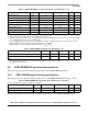
7.1 Enhanced local bus DC electrical characteristics
The following table provides the DC electrical characteristics for the enhanced local bus interface.
7.2 Enhanced local bus AC electrical specifications
The following table describes the general timing parameters of the enhanced local bus interface of
MPC8309.
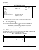
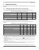
Table 17. Enhanced local bus DC electrical characteristics
Parameter Symbol Min Max Unit
High-level input voltage V
IH
2OV
DD
+0.3 V
Low-level input voltage V
IL
–0.3 0.8 V
High-level output voltage, I
OH
= –100 μAV
OH
OV
DD
–0.2 — V
Low-level output voltage, I
OL
=100μAV
OL
—0.2V
Input current I
IN
—±5μA
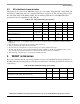
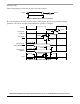
Table 18. Enhanced local bus general timing parameters
Parameter Symbol
1
Min Max Unit Note
Local bus cycle time t
LBK
15 — ns 2
Input setup to local bus clock (LCLK
n
)t
LBIVKH
7—ns3, 4
Input hold from local bus clock (LCLK
n
)t
LBIXKH
1.0 — ns 3, 4
Local bus clock (LCLK
n
) to output valid t
LBKHOV
—3ns3
Local bus clock (LCLK
n
) to output high impedance for LAD/LDP t
LBKHOZ
—4ns5
LALE output fall to LAD output transition (LATCH hold time) t
LBOTOT
3—ns—
LALE output rise to LCLK negative edge t
LALEHOV
—3ns—
LALE output fall to LCLK negative edge t
LALETOT
–5.0 — ns —
Notes:
1. The symbols used for timing specifications follow the pattern of t
(first two letters of functional block)(signal)(state)(reference)(state)
for
inputs and t
(first two letters of functional block)(reference)(state)(signal)(state)
for outputs. For example, t
LBIXKH1
symbolizes local bus
timing (LB) for the input (I) to go invalid (X) with respect to the time the t
LBK
clock reference (K) goes high (H), in this case for
clock one(1).
2. All timings are in reference to falling edge of LCLK0 (for all outputs and for LGTA
and LUPWAIT inputs) or rising edge of
LCLK0 (for all other inputs).
3. All signals are measured from OV
DD
/2 of the rising/falling edge of LCLK0 to 0.4 × OV
DD
of the signal in question for 3.3-V
signaling levels.
4. Input timings are measured at the pin.
5. For purposes of active/float timing measurements, the Hi-Z or off state is defined to be when the total current delivered
through the component pin is less than or equal to the leakage current specification.