
Datasheet

MPC8309 PowerQUICC II Pro Integrated Communications Processor Family Hardware Specifications, Rev. 2
18 Freescale Semiconductor
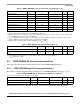
DDR2 SDRAM
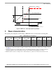
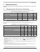
The following figure shows the DDR SDRAM output timing for the MCK to MDQS skew measurement
(t
DDKHMH
).
Figure 5. Timing diagram for t
DDKHMH
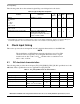
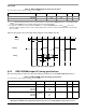
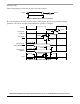
The following figure shows the DDR2 SDRAM output timing diagram.
Figure 6. DDR2 SDRAM output timing diagram
MDQS
MCK
MCK
t
MCK
MDQS
t
DDKHMH
(max) = 0.6 ns
t
DDKHMH
(min) = –0.6 ns
ADDR/CMD
t
DDKHAS
,t
DDKHCS
t
DDKHMH
t
DDKLDS
t
DDKHDS
MDQ[x]/
MDQS[n]
MCK
[n]
MCK[n]
t
MCK
t
DDKLDX
t
DDKHDX
D1D0
t
DDKHAX
,t
DDKHCX
Write A0 NOOP
t
DDKHME
t
DDKHMP
MECC[x]