
Datasheet

MPC8309 PowerQUICC II Pro Integrated Communications Processor Family Hardware Specifications, Rev. 2
16 Freescale Semiconductor
DDR2 SDRAM
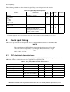
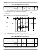
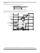
The following figure shows the input timing diagram for the DDR controller.
Figure 4. DDR input timing diagram
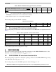
6.2.2 DDR2 SDRAM output AC timing specifications
The following table provides the output AC timing specifications for the DDR2 SDRAM interfaces.
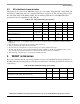
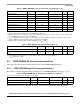
Table 15. DDR2 SDRAM input AC timing specifications
At recommended operating conditions with GV
DD
of 1.8V ± 100mV.
Parameter Symbol Min Max Unit Note
Controller skew for MDQS—MDQ/MDM t
CISKEW
ps 1, 2
266 MHz –750 750
Notes:
1. t
CISKEW
represents the total amount of skew consumed by the controller between MDQS[n] and any corresponding bit that
is captured with MDQS[n]. This should be subtracted from the total timing budget.
2. The amount of skew that can be tolerated from MDQS to a corresponding MDQ signal is called t
DISKEW
. This can be
determined by the equation: t
DISKEW
= ±(T/4 – abs(t
CISKEW
)) where T is the clock period and abs(t
CISKEW
) is the absolute
value of t
CISKEW
.
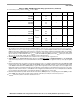
Table 16. DDR2 SDRAM output AC timing specifications
At recommended operating conditions with GV
DD
of 1.8V ± 100mV.
Parameter Symbol
1
Min Max Unit Note
MCK cycle time, (MCK/MCK
crossing) t
MCK
5.988 8 ns 2
ADDR/CMD output setup with respect to MCK t
DDKHAS
ns 3
333 MHz
266 MHz
2.4
2.5
—
ADDR/CMD output hold with respect to MCK t
DDKHAX
ns 3
333 MHz
266 MHz
2.4
2.5
—
MCK[n]
MCK[n]
t
MCK
MDQ[x]
MDQS[n]
t
DISKEW
D1D0
t
DISKEW