
Datasheet

MPC8309 PowerQUICC II Pro Integrated Communications Processor Family Hardware Specifications, Rev. 2
12 Freescale Semiconductor
Clock input timing
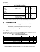
The following table shows the estimated typical I/O power dissipation for the device.
4 Clock input timing
This section provides the clock input DC and AC electrical characteristics for the MPC8309.
NOTE
The rise/fall time on QUICC Engine input pins should not exceed 5 ns. This
should be enforced especially on clock signals. Rise time refers to signal
transitions from 10% to 90% of OV
DD
; fall time refers to transitions from
90% to 10% of OV
DD
.
4.1 DC electrical characteristics
The following table provides the clock input (SYS_CLK_IN/PCI_SYNC_IN) DC specifications for the
MPC8309. These specifications are also applicable for QE_CLK_IN.
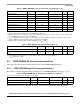
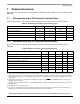
Table 6. Typical I/O power dissipation
Interface Parameter
GV
DD
(1.8 V)
OV
DD
(3.3 V)
Unit Comments
DDR I/O
65% utilization
1.8 V
R
s
= 20 Ω
R
t
= 50 Ω
1 pair of clocks
266 MHz, 1 × 16 bits
0.149
—W —
Local bus I/O load = 25 pF
1 pair of clocks
66 MHz, 26 bits
—0.415W 1
QUICC Engine block and other I/Os TDM serial, HDLC/TRAN serial,
DUART, MII, RMII, Ethernet
management, USB, PCI, SPI, Timer
output, FlexCAN, eSDHC
Note:
1. Typical I/O power is based on a nominal voltage of V
DD
= 3.3V, ambient temperature, and the core running a Dhrystone
benchmark application. The measurements were taken on the evaluation board using WC process silicon.
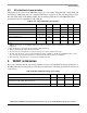
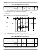
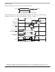
Table 7. SYS_CLK_IN DC electrical characteristics
Parameter Condition Symbol Min Max Unit
Input high voltage — V
IH
2.4 OV
DD
+0.3 V
Input low voltage — V
IL
–0.3 0.4 V
SYS_CLK_IN input current 0 V ≤ V
IN
≤ OV
DD
I
IN
—±5μA
SYS_CLK_IN input current 0 V ≤ V
IN
≤ 0.5 V or
OV
DD
–0.5 V≤ V
IN
≤ OV
DD
I
IN
—±5μA
SYS_CLK_IN input current 0.5 V ≤ V
IN
≤ OV
DD
–0.5 V I
IN
—±50μA