
Datasheet

MPC8309 PowerQUICC II Pro Integrated Communications Processor Family Hardware Specifications, Rev. 2
Freescale Semiconductor 11
Power characteristics
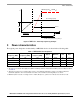
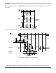
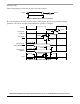
Figure 3. MPC8309 Power-Up sequencing example
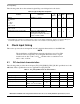
3 Power characteristics
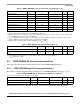
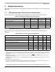
The typical power dissipation for this family of MPC8309 devices is shown in the following table.
Table 5. MPC8309 Power dissipation
Core
Frequency (MHz)
QUICC Engine
Frequency (MHz)
CSB
Frequency (MHz)
Typical Maximum Unit Note
266 233 133 0.341 0.920 W 1, 2, 3
333 233 133 0.361 0.938 W 1, 2, 3
400 233 133 0.381 0.969 W 1,2,3
417 233 167 0.429 1.003 W 1,2,3
Notes:
1. The values do not include I/O supply power (OV
DD
and GV
DD
), but it does include V
DD
and AV
DD
power. For I/O power values,
see Tab l e 6 .
2. Typical power is based on a nominal voltage of V
DD
= 1.0 V, ambient temperature, and the core running a Dhrystone
benchmark application. The measurements were taken on the evaluation board using WC process silicon.
3. Maximum power is based on a voltage of V
DD
= 1.05 V, WC process, a junction T
J
= 105°C, and a smoke test code.
t
90%
V
Core Voltage (V
DD
)
I/O Voltage (GV
DD
and OV
DD
)
0
0.7 V
PORESET
>= 32 × t
SYS_CLK_IN / PCI_SYNC_IN