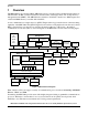
Document Number:MPC8309EC Rev. 2, 09/2012 Freescale Semiconductor Technical Data MPC8309 PowerQUICC II Pro Integrated Communications Processor Family Hardware Specifications This document provides an overview of the MPC8309 PowerQUICC II Pro processor features. The MPC8309 is a cost-effective, highly integrated communications processor that addresses the requirements of several networking applications including residential gateways, modem/routers, industrial control, and test and measurement applications.
Overview 1 Overview The MPC8309 incorporates the e300c3 (MPC 6 03e-based) core built on Power Architecture® technology, which includes 16 KB of each L1 instruction and data caches, dual integer units, and on-chip memory management units (MMUs). The MPC8309 also includes a 32-bit PCI controller, two DMA engines and a 16/32-bit DDR2 memory controller with 8-bit ECC. A new communications complex based on QUICC Engine technology forms the heart of the networking capability of the MPC8309.
Overview 1.
Overview • • • For more information on QUICC Engine sub-modules, see QUICC Engine Block Reference Manual with Protocol Interworking.
Overview • • — External and internal interrupts directed to host processor — Unique vector number for each interrupt source PCI interface — Designed to comply with PCI Local Bus Specification, Revision 2.3 — 32-bit PCI interface operating at up to 66 MHz — PCI 3.
Overview • • • • • — Supports 1-/4-bit SD and SDIO modes, 1-/4-bit modes – Up to 133 Mbps data transfer for SD/SDIO/MMC cards using 4 parallel data lines — Supports block sizes of 1 ~ 4096 bytes Universal serial bus (USB) dual-role controller — Designed to comply with Universal Serial Bus Revision 2.0 Specification — Supports operation as a stand-alone USB host controller — Supports operation as a stand-alone USB device — Supports high-speed (480-Mbps), full-speed (12-Mbps), and low-speed (1.
Electrical characteristics • • • • • • • • 2 Direct memory access (DMA) controller (DMA Engine 2) — Four independent fully programmable DMA channels — Concurrent execution across multiple channels with programmable bandwidth control — Misaligned transfer capability for source/destination address — Data chaining and direct mode — Interrupt on completed segment, error, and chain DUART — Supports 2 DUART — Each has two 2-wire interfaces (RxD, TxD) – The same can be configured as one 4-wire interface (
Electrical characteristics 2.1 Overall DC electrical characteristics This section covers the ratings, conditions, and other characteristics. 2.1.1 Absolute maximum ratings The following table provides the absolute maximum ratings. Table 1. Absolute maximum ratings1 Characteristic Symbol Max Value Unit Notes Core supply voltage VDD –0.3 to 1.26 V — PLL supply voltage AVDD1 AVDD2 AVDD3 –0.3 to 1.26 V — DDR2 DRAM I/O voltage GVDD –0.3 to 1.
Electrical characteristics 2.1.2 Power supply voltage specification The following table provides the recommended operating conditions for the MPC8309. Note that these values are the recommended and tested operating conditions. Proper device operation outside of these conditions is not guaranteed. Table 2. Recommended operating conditions Symbol Recommended Value Unit Note Core supply voltage VDD 1.0 V ± 50 mV V 1 PLL supply voltage AVDD1 AVDD2 AVDD3 1.
Electrical characteristics 2.1.3 Output driver characteristics The following table provides information on the characteristics of the output driver strengths. Table 3. Output drive capability Output Impedance (Ω) Supply Voltage (V) Local bus interface utilities signals 42 OVDD = 3.3 PCI Signal 25 DDR2 signal 18 GVDD = 1.8 DUART, system control, I2C, SPI, JTAG 42 OVDD = 3.3 GPIO signals 42 OVDD = 3.3 Driver Type 2.1.
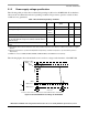
Power characteristics I/O Voltage (GVDD and OVDD) V Core Voltage (VDD) 0.7 V 90% t 0 PORESET >= 32 × tSYS_CLK_IN / PCI_SYNC_IN Figure 3. MPC8309 Power-Up sequencing example 3 Power characteristics The typical power dissipation for this family of MPC8309 devices is shown in the following table. Table 5. MPC8309 Power dissipation Core Frequency (MHz) QUICC Engine Frequency (MHz) CSB Frequency (MHz) Typical Maximum Unit Note 266 233 133 0.341 0.920 W 1, 2, 3 333 233 133 0.361 0.
Clock input timing The following table shows the estimated typical I/O power dissipation for the device. Table 6. Typical I/O power dissipation Interface GVDD (1.8 V) Parameter DDR I/O 65% utilization 1.8 V Rs = 20 Ω Rt = 50 Ω 1 pair of clocks 266 MHz, 1 × 16 bits Local bus I/O load = 25 pF 1 pair of clocks 66 MHz, 26 bits QUICC Engine block and other I/Os TDM serial, HDLC/TRAN serial, DUART, MII, RMII, Ethernet management, USB, PCI, SPI, Timer output, FlexCAN, eSDHC OVDD (3.
RESET initialization 4.2 AC electrical characteristics The primary clock source for the MPC8309 can be one of two inputs, SYS_CLK_IN or PCI_SYNC_IN, depending on whether the device is configured in PCI host or agent mode. The following table provides the clock input (SYS_CLK_IN/PCI_SYNC_IN) AC timing specifications for the MPC8309. These specifications are also applicable for QE_CLK_IN. Table 8. SYS_CLK_IN AC timing specifications Parameter/Condition Symbol Min Typical Max Unit Note 66.
DDR2 SDRAM Table 9. RESET initialization timing specifications (continued) Input setup time for POR configuration signals (CFG_RESET_SOURCE[0:3]) with respect to negation of PORESET 4 — tSYS_CLK_IN Input hold time for POR config signals with respect to negation of HRESET 0 — ns 1, 2 1, 2 Notes: 1. tSYS_CLK_IN is the clock period of the input clock applied to SYS_CLK_IN. For more details, see the MPC8309 PowerQUICC II Pro Integrated Communications Processor Family Reference Manual. 2.
DDR2 SDRAM Table 12. DDR2 SDRAM DC electrical characteristics for GVDD(typ) = 1.8 V Parameter/Condition Symbol Min Max Unit Note GVDD 1.7 1.9 V 1 MVREF 0.49 × GVDD 0.51 × GVDD V 2 I/O termination voltage VTT MVREF – 0.04 MVREF + 0.04 V 3 Input high voltage VIH MVREF+ 0.125 GVDD + 0.3 V — Input low voltage VIL –0.3 MVREF – 0.125 V — Output leakage current IOZ –9.9 9.9 μA 4 Output high current (VOUT = 1.35 V) IOH –13.4 — mA — Output low current (VOUT = 0.
DDR2 SDRAM Table 15. DDR2 SDRAM input AC timing specifications At recommended operating conditions with GV DD of 1.8V ± 100mV. Parameter Symbol Controller skew for MDQS—MDQ/MDM Min Max tCISKEW 266 MHz –750 Unit Note ps 1, 2 750 Notes: 1. tCISKEW represents the total amount of skew consumed by the controller between MDQS[n] and any corresponding bit that is captured with MDQS[n]. This should be subtracted from the total timing budget. 2.
DDR2 SDRAM Table 16. DDR2 SDRAM output AC timing specifications (continued) At recommended operating conditions with GVDD of 1.8V ± 100mV. Symbol1 Parameter MCS output setup with respect to MCK Min Max tDDKHCS 333 MHz 266 MHz MCS output hold with respect to MCK 2.4 2.5 — 2.4 2.5 — –0.6 0.6 tDDKHCX 333 MHz 266 MHz MCK to MDQS Skew tDDKHMH MDQ/MDM output setup with respect to MDQS tDDKHDS, tDDKLDS 333 MHz 266 MHz MDQ/MDM output hold with respect to MDQS 0.8 0.
DDR2 SDRAM The following figure shows the DDR SDRAM output timing for the MCK to MDQS skew measurement (tDDKHMH). MCK MCK tMCK tDDKHMH(max) = 0.6 ns MDQS tDDKHMH(min) = –0.6 ns MDQS Figure 5. Timing diagram for tDDKHMH The following figure shows the DDR2 SDRAM output timing diagram. MCK[n] MCK[n] tMCK tDDKHAS ,tDDKHCS tDDKHAX ,tDDKHCX ADDR/CMD Write A0 NOOP tDDKHMP tDDKHMH MDQS[n] tDDKHME tDDKHDS tDDKLDS MDQ[x]/ MECC[x] D0 D1 tDDKLDX tDDKHDX Figure 6.
Enhanced local bus 7 Enhanced local bus This section describes the DC and AC electrical specifications for the enhanced local bus interface of the MPC8309. 7.1 Enhanced local bus DC electrical characteristics The following table provides the DC electrical characteristics for the enhanced local bus interface. Table 17. Enhanced local bus DC electrical characteristics Parameter Symbol Min Max Unit High-level input voltage VIH 2 OVDD + 0.3 V Low-level input voltage VIL –0.3 0.
Enhanced local bus The following figure provides the AC test load for the local bus. Output Z0 = 50 Ω OVDD/2 RL = 50 Ω Figure 7. Enhanced local bus ac test load The following figures show the local bus signals. These figures have been given indicate timing parameters only and do not reflect actual functional operation of interface.
Enhanced local bus LCLK T1 T3 tLBKHOV tLBKHOZ GPCM Mode Output Signals: LCS[0:3]/LWE tLBIVKH tLBIXKH UPM Mode Input Signal: LUPWAIT tLBIVKH tLBIXKH Input Signals: LAD[0:15]/LDP[0:3] tLBKHOV tLBKHOZ UPM Mode Output Signals: LCS[0:3]/LBS[0:1]/LGPL[0:5] Figure 9. Enhanced local bus signals, GPCM/UPM signals for LCRR[CLKDIV] = 2 MPC8309 PowerQUICC II Pro Integrated Communications Processor Family Hardware Specifications, Rev.
Ethernet and MII management LCLK T1 T2 T3 T4 tLBKHOV tLBKHOZ GPCM Mode Output Signals: LCS[0:3]/LWE tLBIVKH tLBIXKH UPM Mode Input Signal: LUPWAIT tLBIXKH tLBIVKH Input Signals: LAD[0:15] tLBKHOV tLBKHOZ UPM Mode Output Signals: LCS[0:3]/LBS[0:1]/LGPL[0:5] Figure 10. Enhanced local bus signals, GPCM/UPM Signals for LCRR[CLKDIV] = 4 8 Ethernet and MII management This section provides the AC and DC electrical characteristics for Ethernet interfaces. 8.
Ethernet and MII management Table 19. MII and RMII DC electrical characteristics Parameter Symbol Conditions Min Max Unit Supply voltage 3.3 V OVDD — 3 3.6 V Output high voltage VOH IOH = –4.0 mA OVDD = Min 2.40 OVDD + 0.3 V Output low voltage VOL IOL = 4.0 mA OVDD = Min GND 0. Input high voltage VIH — — 2.0 OVDD + 0.3 V Input low voltage VIL — — –0.3 0.90 V Input current IIN 0 V ≤ VIN ≤ OVDD — ±5 μA 8.
Ethernet and MII management The following figure provides the AC test load. Output Z0 = 50 Ω RL = 50 Ω OVDD/2 Figure 11. AC test load The following figure shows the MII transmit AC timing diagram. tMTXR tMTX TX_CLK tMTXH tMTXF TXD[3:0] TX_EN TX_ER tMTKHDX Figure 12. MII transmit AC timing diagram 8.2.1.2 MII receive AC timing specifications The following table provides the MII receive AC timing specifications. Table 21.
Ethernet and MII management The following figure shows the MII receive AC timing diagram. tMRXR tMRX RX_CLK tMRXH RXD[3:0] RX_DV RX_ER tMRXF Valid Data tMRDVKH tMRDXKH Figure 13. MII receive AC timing diagram 8.2.2 RMII AC timing specifications This section describes the RMII transmit and receive AC timing specifications. 8.2.2.1 RMII transmit AC timing specifications The following table provides the RMII transmit AC timing specifications. Table 22.
Ethernet and MII management The following figure shows the RMII transmit AC timing diagram. tRMX tRMXR REF_CLK tRMXH tRMXF TXD[1:0] TX_EN tRMTKHDX Figure 15. RMII transmit AC timing diagram 8.2.2.2 RMII receive AC timing specifications The following table provides the RMII receive AC timing specifications. Table 23. RMII receive AC timing specifications At recommended operating conditions with OVDD of 3.3 V ± 300mV.
Ethernet and MII management The following figure shows the RMII receive AC timing diagram. tRMXR tRMX REF_CLK tRMXH tRMXF RXD[1:0] CRS_DV RX_ER Valid Data tRMRDVKH tRMRDXKH Figure 16. RMII receive AC timing diagram 8.3 Ethernet management interface electrical characteristics The electrical characteristics specified here apply to MII management interface signals MDIO (management data input/output) and MDC (management data clock).
Ethernet and MII management Table 25. MII management AC timing specifications (continued) At recommended operating conditions with OVDD is 3.3 V ± 300mV. Symbol1 Min Typical Max Unit Note MDC to MDIO delay tMDKHDX 10 — 70 ns — MDIO to MDC setup time tMDDVKH 8.5 — — ns — MDIO to MDC hold time tMDDXKH 0 — — ns — MDC rise time tMDCR — — 10 ns — MDC fall time tMDHF — — 10 ns — Parameter/Condition Note: 1.
TDM/SI 9 TDM/SI This section describes the DC and AC electrical specifications for the time-division-multiplexed and serial interface of the MPC8309. 9.1 TDM/SI DC electrical characteristics The following table provides the DC electrical characteristics for the MPC8309 TDM/SI. Table 26. TDM/SI DC electrical characteristics Characteristic Symbol Condition Min Max Unit Output high voltage VOH IOH = –2.0 mA 2.4 — V Output low voltage VOL IOL = 3.2 mA — 0.
HDLC The following figure represents the AC timing from Table 27. Note that although the specifications generally reference the rising edge of the clock, these AC timing diagrams also apply when the falling edge is the active edge. TDM/SICLK (Input) Input Signals: TDM/SI (See Note) tSEIXKH tSEIVKH tSEKHOV Output Signals: TDM/SI (See Note) tSEKHOX Note: The clock edge is selectable on TDM/SI. Figure 19.
HDLC Table 29. HDLC AC timing specifications1 (continued) Symbol2 Min Max Unit tHEKHOX 1 8 ns Inputs—Internal clock input setup time tHIIVKH 9 — ns Inputs—External clock input setup time tHEIVKH 4 — ns Inputs—Internal clock input hold time tHIIXKH 0 — ns Inputs—External clock input hold time tHEIXKH 1 — ns Characteristic Outputs—External clock high impedance Notes: 1.
PCI The following figure shows the timing with internal clock. Serial CLK (Output) tHIIXKH tHIIVKH Input Signals: (See Note) tHIKHOV Output Signals: (See Note) tHIKHOX Note: The clock edge is selectable. Figure 22. AC timing (internal clock) diagram 11 PCI This section describes the DC and AC electrical specifications for the PCI bus of the MPC8309. 11.1 PCI DC electrical characteristics Table 30 provides the DC electrical characteristics for the PCI interface of the MPC8309. Table 30.
PCI Table 31. PCI AC timing specifications at 66 MHz Symbol1 Min Max Unit Notes Clock to output valid tPCKHOV — 6.0 ns 2 Output hold from clock tPCKHOX 1 — ns 2 Clock to output high impedance tPCKHOZ — 14 ns 2, Input setup to clock tPCIVKH 3.0 — ns 2, 4 Input hold from clock tPCIXKH 0 — ns 2, Parameter 3 4 Notes: 1.
USB Figure 24 shows the PCI input AC timing conditions. CLK tPCIVKH tPCIXKH Input Figure 24. PCI input AC timing measurement conditions Figure 25 shows the PCI output AC timing conditions. CLK tPCKHOV tPCKHOX Output Delay tPCKHOZ High-Impedance Output Figure 25. PCI output AC timing measurement condition 12 USB 12.1 USB controller This section provides the AC and DC electrical specifications for the USB (ULPI) interface. 12.1.
USB Table 34. USB general timing parameters Symbol1 Min Max Unit Note tUSCK 15 — ns — Input setup to USB clock—all inputs tUSIVKH 4 — ns — input hold to USB clock—all inputs tUSIXKH 1 — ns — USB clock to output valid—all outputs (except USBDR_STP_USBDR_STP) tUSKHOV — 7 ns — USB clock to output valid—USBDR_STP tUSKHOV — 7.5 ns — Output hold from USB clock—all outputs tUSKHOX 2 — ns — Parameter USB clock cycle time Note: 1.
DUART 13 DUART This section describes the DC and AC electrical specifications for the DUART interface of the MPC8309. 13.1 DUART DC electrical characteristics The following table provides the DC electrical characteristics for the DUART interface of the MPC8309. Table 35. DUART DC electrical characteristics Parameter Symbol Min Max Unit High-level input voltage VIH 2 OVDD + 0.3 V Low-level input voltage OVDD VIL –0.3 0.8 V High-level output voltage, IOH = –100 μA VOH OVDD – 0.
eSDHC 14 eSDHC This section describes the DC and AC electrical specifications for the eSDHC interface of the device. 14.1 eSDHC DC electrical characteristics The following table provides the DC electrical characteristics for the eSDHC interface. Table 37. eSDHC Interface DC electrical characteristics At recommended operating conditions with OVDD = 3.3 V Characteristic Symbol Condition Min Max Unit Note Input high voltage VIH — 0.625 × OVDD — V 1 Input low voltage VIL — — 0.
eSDHC Table 38. eSDHC AC timing specifications (continued) At recommended operating conditions with OVDD = 3.3 V Symbol1 Min Max Unit Notes Input hold times: SD_CMD, SD_DATx, SD_CD to SD_CLK tSHSIXKH 2.5 — ns 3, 4 Output delay time: SD_CLK to SD_CMD, SD_DATx valid tSHSKHOV –3 3 ns 4 Parameter Notes: 1.
FlexCAN 15 FlexCAN This section describes the DC and AC electrical specifications for the FlexCAN interface. 15.1 FlexCAN DC electrical characteristics The following table provides the DC electrical characteristics for the FlexCAN interface. Table 39. FlexCAN DC electrical characteristics (3.3V) For recommended operating conditions, see Table 2 Parameter Symbol Min Max Unit Notes Input high voltage VIH 2 — V 1 Input low voltage VIL — 0.
I2C 16 I2C This section describes the DC and AC electrical characteristics for the I2C interface of the MPC8309. 16.1 I2C DC electrical characteristics The following table provides the DC electrical characteristics for the I2C interface of the MPC8309. Table 41. I2C DC electrical characteristics At recommended operating conditions with OVDD of 3.3 V ± 300mV. Parameter Symbol Min Max Unit Notes Input high voltage level VIH 0.7 × OVDD OVDD + 0.3 V — Input low voltage level VIL –0.3 0.
I2C Table 42. I2C AC electrical specifications (continued) All values refer to VIH (min) and VIL (max) levels (see Table 41). Symbol1 Min Max Unit tI2CF 20 + 0.1 C B4 300 ns Setup time for STOP condition tI2PVKH 0.6 — μs Bus free time between a STOP and START condition tI2KHDX 1.3 — μs Noise margin at the LOW level for each connected device (including hysteresis) VNL 0.1 × OVDD — V Noise margin at the HIGH level for each connected device (including hysteresis) VNH 0.
Timers 17 Timers This section describes the DC and AC electrical specifications for the timers of the MPC8309. 17.1 Timer DC electrical characteristics The following table provides the DC electrical characteristics for the MPC8309 timer pins, including TIN, TOUT, TGATE, and RTC_PIT_CLK. Table 43. Timer DC electrical characteristics Characteristic Symbol Condition Min Max Unit 4 — V Output high voltage VOH Output low voltage VOL IOL = 6.0 mA — 0.5 V Output low voltage VOL IOL = 3.
GPIO 18 GPIO This section describes the DC and AC electrical specifications for the GPIO of the MPC8309. 18.1 GPIO DC electrical characteristics The following table provides the DC electrical characteristics for the MPC8309 GPIO. Table 45. GPIO DC electrical characteristics Characteristic Symbol Condition Min Max Unit Notes Output high voltage VOH IOH = –6.0 mA 2.4 — V 1 Output low voltage VOL IOL = 6.0 mA — 0.5 V 1 Output low voltage VOL IOL = 3.2 mA — 0.
IPIC 19 IPIC This section describes the DC and AC electrical specifications for the external interrupt pins of the MPC8309. 19.1 IPIC DC electrical characteristics The following table provides the DC electrical characteristics for the external interrupt pins of the MPC8309. Table 47. IPIC DC electrical characteristics1,2 Characteristic Symbol Condition Min Max Unit Input high voltage VIH — 2.0 OVDD + 0.3 V Input low voltage VIL — –0.3 0.
SPI Table 49. SPI DC electrical characteristics Characteristic Symbol Condition Min Max Unit Output high voltage VOH IOH = –6.0 mA 2.4 — V Output low voltage VOL IOL = 6.0 mA — 0.5 V Output low voltage VOL IOL = 3.2 mA — 0.4 V Input high voltage VIH — 2.0 OVDD + 0.3 V Input low voltage VIL — –0.3 0.8 V Input current IIN 0 V ≤ VIN ≤ OVDD 5 μA 20.2 —± SPI AC timing specifications The following table and provide the SPI input and output AC timing specifications.
JTAG The following figure shows the SPI timing in slave mode (external clock). SPICLK (Input) Input Signals: SPIMOSI (See Note) tNEIXKH tNEIVKH tNEKHOV Output Signals: SPIMISO (See Note) Note: The clock edge is selectable on SPI. Figure 35. SPI AC Timing in slave mode (external clock) diagram The following figure shows the SPI timing in master mode (internal clock).
JTAG Table 51. JTAG interface DC electrical characteristics (continued) Characteristic Symbol Condition Min Max Unit Input high voltage VIH — 2.0 OVDD + 0.3 V Input low voltage VIL — –0.3 0.8 V Input current IIN 0 V ≤ VIN ≤ OVDD — ±5 μA 21.2 JTAG AC electrical characteristics This section describes the AC electrical specifications for the IEEE Std. 1149.1 (JTAG) interface of the MPC8309.
JTAG Table 52. JTAG AC timing specifications (independent of SYS_CLK_IN) 1 (continued) At recommended operating conditions (see Table 2). Symbol2 Min Max Boundary-scan data TDO tJTKLDX tJTKLOX 2 2 — — JTAG external clock to output high impedance: Boundary-scan data TDO tJTKLDZ tJTKLOZ 2 2 19 9 Parameter Unit Notes ns Output hold times: 5 ns 5, 6 6 Notes: 1. All outputs are measured from the midpoint voltage of the falling/rising edge of tTCLK to the midpoint of the signal in question.
JTAG The following figure provides the boundary-scan timing diagram. JTAG External Clock VM VM tJTDVKH tJTDXKH Input Data Valid Boundary Data Inputs tJTKLDV tJTKLDX Boundary Data Outputs Output Data Valid tJTKLDZ Boundary Data Outputs Output Data Valid VM = Midpoint Voltage (OVDD/2) Figure 40. Boundary-Scan timing diagram The following figure provides the test access port timing diagram.
Package and pin listings 22 Package and pin listings This section details package parameters, pin assignments, and dimensions. The MPC8309 is available in a thermally enhanced MAPBGA (mold array process-ball grid array); see Section 22.1, “Package parameters for the MPC8309,” and Section 22.2, “Mechanical dimensions of the MPC8309 MAPBGA,” for information on the MAPBGA. 22.1 Package parameters for the MPC8309 The package parameters are as provided in the following list.
Package and pin listings Figure 42. Mechanical dimensions and bottom surface nomenclature of the MPC8309 MAPBGA Notes: 1. All dimensions are in millimeters. 2. Dimensions and tolerances per ASME Y14.5M-1994. 3. Maximum solder ball diameter measured parallel to datum A. 4. Datum A, the seating plane, is determined by the spherical crowns of the solder balls. MPC8309 PowerQUICC II Pro Integrated Communications Processor Family Hardware Specifications, Rev.
Package and pin listings 22.3 Pinout listings Following table shows the pin list of the MPC8309. Table 53.
Package and pin listings MEMC_MDQ29 D2 IO GVDD — MEMC_MDQ30 C2 IO GVDD — MEMC_MDQ31 C1 IO GVDD — MEMC_MECC0 Y5 IO GVDD — MEMC_MECC1 AA4 IO GVDD — MEMC_MECC2 Y4 IO GVDD — MEMC_MECC3 AA3 IO GVDD — MEMC_MECC4 AC2 IO GVDD — MEMC_MECC5 AB2 IO GVDD — MEMC_MECC6 Y3 IO GVDD — MEMC_MECC7 AB1 IO GVDD — MEMC_MDM0 W1 O GVDD — MEMC_MDM1 E1 O GVDD — MEMC_MDM2 V3 O GVDD — MEMC_MDM3 D1 O GVDD — MEMC_MDM8 W5 O GVDD — MEMC_MDQS0 T5 IO GVDD —
Package and pin listings MEMC_MA13 P1 O GVDD - MEMC_MWE_B J1 O GVDD - MEMC_MRAS_B K1 O GVDD - MEMC_MCAS_B J3 O GVDD - MEMC_MCS_B0 J4 O GVDD - MEMC_MCS_B1 K5 O GVDD - MEMC_MCKE P4 O GVDD - MEMC_MCK0 R1 O GVDD - MEMC_MCK1 R3 O GVDD - MEMC_MCK_B0 T1 O GVDD - MEMC_MCK_B1 P3 O GVDD - MEMC_MODT0 H1 O GVDD - MEMC_MODT1 H2 O GVDD - MEMC_MVREF M6 GVDD - Local Bus Controller Interface LAD0 B5 IO OVDD - LAD1 A4 IO OVDD - LAD2 C7 IO OVDD
Package and pin listings LA22 A11 O OVDD - LA23 A10 O OVDD - LA24 C12 O OVDD - LA25 A12 O OVDD - LCLK0 E13 O OVDD - LCS_B0 D13 O OVDD 2 LCS_B1 C13 O OVDD 2 LCS_B2 A13 O OVDD 2 LCS_B3 B13 O OVDD 2 LWE_B0/LFWE_B0/LBS_B0 A14 O OVDD - LWE_B1/LBS_B1 B14 O OVDD - LBCTL A15 O OVDD - LGPL0/LFCLE C14 O OVDD - LGPL1/LFALE C15 O OVDD - LGPL2/LOE_B/LFRE_B B16 O OVDD 2 LGPL3/LFWP_B A16 O OVDD - LGPL4/LGTA_B/LUPWAIT/LFRB_B E14 IO OVDD 2
Package and pin listings SPIMISO E16 SPICLK E17 SPISEL A19 SPISEL_BOOT_B D18 IO OVDD - IO OVDD - I OVDD - OVDD - JTAG TCK A2 I OVDD - TDI C5 I OVDD 2 TDO A3 O OVDD - TMS D7 I OVDD 2 TRST_B E9 I OVDD 2 I OVDD - Test Interface TEST_MODE C6 System Control Signals HRESET_B W23 IO OVDD 1 PORESET_B W22 I OVDD - Clock Interface QE_CLK_IN R22 I OVDD - SYS_CLK_IN R23 I OVDD - SYS_XTAL_IN P23 I OVDD - SYS_XTAL_OUT P19 O OVDD - PCI_SYNC_IN
Package and pin listings GPIO_9/TXCAN1/LSRCID1/LCS_B5 C17 IO OVDD - GPIO_10/RXCAN2/LSRCID2/LCS_B6 E15 IO OVDD - GPIO_11/TXCAN2/LSRCID3/LCS_B7 A18 IO OVDD - GPIO_12/RXCAN3/LSRCID4/LCLK1 D15 IO OVDD - GPIO_13/TXCAN3/LDVAL C18 IO OVDD - GPIO_14/RXCAN4 D16 IO OVDD - GPIO_15/TXCAN4 C19 IO OVDD - USB USBDR_PWRFAULT/CE_PIO_1 AA6 I OVDD 1 USBDR_CLK/UART2_SIN2/UART2_CTS_B1 AC9 I OVDD - USBDR_DIR AA7 I OVDD - USBDR_NXT/UART2_SIN1/QE_EXT_REQ_4 AC5 I OVDD - USBDR_
Package and pin listings PCI_AD8/ E21 IO OVDD - PCI_AD9/ H20 IO OVDD - PCI_AD10/ D22 IO OVDD - PCI_AD11/ D23 IO OVDD - PCI_AD12/ J19 IO OVDD - PCI_AD13/ F21 IO OVDD - PCI_AD14/ G21 IO OVDD - PCI_AD15/ E22 IO OVDD - PCI_AD16/ E23 IO OVDD - PCI_AD17/ J20 IO OVDD - PCI_AD18/ F23 IO OVDD - PCI_AD19/ G23 IO OVDD - PCI_AD20 K19 IO OVDD - PCI_AD21 H21 IO OVDD - PCI_AD22 L19 IO OVDD - PCI_AD23 G22 IO OVDD - PCI_AD24 H23 IO OVDD -
Package and pin listings PCI_REQ_B0 P21 IO OVDD - PCI_REQ_B1/CPCI_HS_ES P22 IO OVDD - PCI_REQ_B2 T22 IO OVDD - PCI_GNT_B0 T21 IO OVDD - PCI_GNT_B1/CPCI_HS_LED U22 O OVDD - PCI_GNT_B2/CPCI_HS_ENUM U21 IO OVDD - M66EN V21 I OVDD - PCI_CLK0 T19 O OVDD - PCI_CLK1 U19 O OVDD - PCI_CLK2 R19 O OVDD - Ethernet Management FEC_MDC W18 O OVDD - FEC_MDIO W17 IO OVDD - Y18 IO OVDD - FEC1_CRS/GTM1_TGATE1_B/GPIO_17 AA19 IO OVDD - FEC1_RX_CLK[CLK9]/GPIO_1
Package and pin listings FEC2_RX_CLK[CLK7]/GPIO_34 W14 IO OVDD - FEC2_RX_DV/GTM2_TIN2/GPIO_35 AB16 IO OVDD - Y14 IO OVDD - FEC2_RXD0/GPIO_37 AA15 IO OVDD - FEC2_RXD1/GTM2_TIN3/GPIO_38 AC15 IO OVDD - FEC2_RXD2/GTM2_TGATE3_B/GPIO_39 AC16 IO OVDD - FEC2_RXD3/GPIO_40 AA14 IO OVDD - FEC2_TX_CLK[CLK8]/GTM2_TIN4/GPIO_41 W13 IO OVDD - FEC2_TX_EN/GTM2_TGATE4_B/GPIO_42 AB14 IO OVDD - FEC2_TX_ER/GTM2_TOUT4_B/GPIO_43 AC14 IO OVDD - FEC2_TXD0/GTM2_TOUT1_B/GPIO_44 Y12 I
Package and pin listings HDLC/TDM/GPIO HDLC1_TXCLK[CLK16]/GPIO_0/QE_BRG_5/TD M1_TCK[CLK4] AA20 IO OVDD - HDLC1_RXCLK[CLK15]/GPIO_1/TDM1_RCK [CLK3] AA21 IO OVDD - HDLC1_TXD/GPIO_2/TDM1_TD/CFG_RESET_ SOURCE[0] AB22 IO OVDD 1 HDLC1_RXD/GPIO_3/TDM1_RD AB23 IO OVDD - HDLC1_CD_B/GPIO_4/TDM1_TFS W19 IO OVDD - HDLC1_CTS_B/GPIO_5/TDM1_RFS V19 IO OVDD - HDLC1_RTS_B/GPIO_6/TDM1_STROBE_B/CF G_RESET_SOURCE[1] AA23 IO OVDD - HDLC2_TXCLK[CLK14]/GPIO_16/QE_BRG_7/T DM2_TCK[CLK6] Y20 IO
Package and pin listings VDD H8,H9,H10,H11,H12,M8, H13,N16,H14,H15,H16, P16,P8,L8,K16,J16,K8,J 8,R8,T16,R16,T8,T9,T11 ,T10,T12,T13,T14,T15 - - - VSS A1, C3, F22, J14, K14, M15, L15, N20, R9, Y21, T20, AB21, B1, C22,G4, K15, J15, M2, M22, P9, R10, V2, AA2, AC1, B4,D5, G20, J22, K20, M5, N9, P10, R11, V22, AA22,AC23, B6, D8, J2, K4, M9,L9, N10, P11, R12, W4, AB4, D11, B9, J9, K9, L10,M10, N11, P12, R13, Y7,AB6, B12, D14, J10, K10, L11, M11, P13, N12, R14, Y10,AB9, B15, D17, J11, K11, D20, B18, J12, K12
Clocking 23 Clocking The following figure shows the internal distribution of clocks within the MPC8309.
Clocking 23.1 Clocking in PCI host mode When the MPC8309 is configured as a PCI host device (RCWH[PCIHOST] = 1), SYS_CLK_IN is its primary input clock. SYS_CLK_IN feeds the PCI clock divider (÷2) and the PCI_SYNC_OUT and PCI_CLK multiplexors. The CFG_CLKIN_DIV configuration input selects whether SYS_CLK_IN or SYS_CLK_IN/2 is driven out on the PCI_SYNC_OUT signal. PCI_SYNC_OUT is connected externally to PCI_SYNC_IN to allow the internal clock subsystem to synchronize to the system PCI clocks.
Clocking Configuration chapter in the MPC8309 PowerQUICC II Pro Integrated Communications Processor Family Reference Manual. The qe_clk frequency is determined by the QUICC Engine PLL multiplication factor (RCWL[CEPMF]) and the QUICC Engine PLL division factor (RCWL[CEPDF]) as the following equation: qe_clk = (QE_CLK_IN × CEPMF) ÷ (1 + CEPDF) Eqn.
Clocking Table 55. Operating Frequencies for MAPBGA (continued) Characteristic1 DDR2 memory bus frequency (MCLK)2 3 Local bus frequency (LCLKn) Max Operating Frequency Unit 167 MHz 66 MHz Notes: 1. The SYS_CLK_IN frequency, RCWL[SPMF], and RCWL[COREPLL] settings must be chosen such that the resulting csb_clk, MCLK, LCLK, and core_clk frequencies do not exceed their respective maximum or minimum operating frequencies. 2. The DDR2 data rate is 2× the DDR2 memory bus frequency. 3.
Clocking Table 57. CSB frequency options PCI_SYNC_IN(MHz) SPMF csb_clk : sys_clk_in Ratio 25 33.33 66.67 csb_clk Frequency (MHz) 23.5 0010 2:1 0011 3:1 0100 4:1 0101 5:1 0110 6:1 133 133 125 167 Core PLL configuration RCWL[COREPLL] selects the ratio between the internal coherent system bus clock (csb_clk) and the e300 core clock (core_clk). The following table shows the encodings for RCWL[COREPLL]. COREPLL values not listed, and should be considered reserved. Table 58.
Clocking Table 58. e300 Core PLL configuration (continued) RCWL[COREPLL] 0-1 2-5 core_clk : csb_clk Ratio VCO Divider 6 01 0011 0 3:1 ÷4 10 0011 0 3:1 ÷8 11 0011 0 3:1 ÷8 NOTE Core VCO frequency = core frequency × VCO divider. The VCO divider (RCWL[COREPLL[0:1]]), must be set properly so that the core VCO frequency is in the range of 400–800 MHz. 23.6 QUICC Engine PLL configuration The QUICC Engine PLL is controlled by the RCWL[CEPMF] and RCWL[CEPDF] parameters.
Clocking NOTE The VCO divider (RCWL[CEVCOD]) must be set properly so that the QUICC Engine VCO frequency is in the range of 300–600 MHz. The QUICC Engine frequency is not restricted by the CSB and core frequencies. The CSB, core, and QUICC Engine frequencies should be selected according to the performance requirements.
Thermal 24 Thermal This section describes the thermal specifications of the MPC8309. 24.1 Thermal characteristics The following table provides the package thermal characteristics for the 369, 19 × 19 mm MAPBGA of the MPC8309. Table 62.
Thermal TA = ambient temperature for the package (°C) RθJA = junction-to-ambient thermal resistance (°C/W) PD = power dissipation in the package (W) The junction-to-ambient thermal resistance is an industry standard value that provides a quick and easy estimation of thermal performance. As a general statement, the value obtained on a single layer board is appropriate for a tightly packed printed-circuit board.
Thermal TT = thermocouple temperature on top of package (°C) ΨJT = thermal characterization parameter (°C/W) PD = power dissipation in package (W) The thermal characterization parameter is measured per JESD51-2 specification using a 40 gauge type T thermocouple epoxied to the top center of the package case. The thermocouple should be positioned so that the thermocouple junction rests on the package.
System design information lifetime of the package. Recommended maximum force on the top of the package is 10 lb (4.5 kg) force. If an adhesive attachment is planned, the adhesive should be intended for attachment to painted or plastic surfaces and its performance verified under the application requirements. 24.2.
System design information 25.2 PLL power supply filtering Each of the PLLs listed above is provided with power through independent power supply pins. The voltage level at each AVDDn pin should always be equivalent to VDD, and preferably these voltages are derived directly from VDD through a low frequency filter scheme such as the following.
System design information to minimize inductance. Suggested bulk capacitors—100 to 330 µF (AVX TPS tantalum or Sanyo OSCON). 25.4 Output buffer DC impedance For all buses, the driver is a push-pull single-ended driver type (open drain for I2C). To measure Z0 for the single-ended drivers, an external resistor is connected from the chip pad to OVDD or GND. Then, the value of each resistor is varied until the pad voltage is OVDD/2 (see Figure 45).
Ordering information The following table summarizes the signal impedance targets. The driver impedance is targeted at minimum VDD, nominal OVDD, 105°C. Table 63. Impedance characteristics Impedance Local Bus, Ethernet, DUART, Control, Configuration and Power Management DDR DRAM Symbol Unit RN 42 Target 20 Target Z0 ? RP 42 Target 20 Target Z0 ? Differential NA NA ZDIFF ? Note: Nominal supply voltages. See Table 1, T j = 105°C. 25.
Ordering information Table 64. Part numbering nomenclature MPC nnnn C VM AF D C A Product Code Part Identifier Temperature Range1 Package2 e300 Core Frequency3 DDR2 Frequency QUICC Engine Frequency Revision Level MPC 8309 VM = Pb-free AD = 266 MHz AF = 333 MHz AG = 400 MHz AH = 417MHz Blank = 0 to 105°C C = –40 to 105°C D = 266 MHz F = 333 MHz C = 233 MHz Contact local Freescale sales office Notes: 1. Contact local Freescale office on availability of parts with C temperature range.
Document revision history 27 Document revision history The following table provides a revision history for this document. Table 66. Document revision history Rev. No. Date Substantive Change(s) 2 09/2012 • In Table 53, swapped CLK13 and CLK14.
How to Reach Us: Home Page: www.freescale.com Web Support: http://www.freescale.com/support USA/Europe or Locations Not Listed: Freescale Semiconductor, Inc. Technical Information Center, EL516 2100 East Elliot Road Tempe, Arizona 85284 1-800-521-6274 or +1-480-768-2130 www.freescale.