
Datasheet


Table Of Contents
- MCF5282 and MCF5216 ColdFire® Microcontroller User’s Manual
- About This Book
- Chapter 1 Overview
- 1.1 Key Features
- 1.1.1 Version 2 ColdFire Core
- 1.1.2 System Control Module
- 1.1.3 External Interface Module (EIM)
- 1.1.4 Chip Select
- 1.1.5 Power Management
- 1.1.6 General Input/Output Ports
- 1.1.7 Interrupt Controllers (INTC0/INTC1)
- 1.1.8 SDRAM Controller
- 1.1.9 Test Access Port
- 1.1.10 UART Modules
- 1.1.11 DMA Timers (DTIM0-DTIM3)
- 1.1.12 General-Purpose Timers (GPTA/GPTB)
- 1.1.13 Periodic Interrupt Timers (PIT0-PIT3)
- 1.1.14 Software Watchdog Timer
- 1.1.15 Phase Locked Loop (PLL)
- 1.1.16 DMA Controller
- 1.1.17 Reset
- 1.2 MCF5282-Specific Features
- 1.1 Key Features
- Chapter 2 ColdFire Core
- 2.1 Introduction
- 2.2 Memory Map/Register Description
- 2.2.1 Data Registers (D0-D7)
- 2.2.2 Address Registers (A0-A6)
- 2.2.3 Supervisor/User Stack Pointers (A7 and OTHER_A7)
- 2.2.4 Condition Code Register (CCR)
- 2.2.5 Program Counter (PC)
- 2.2.6 Cache Control Register (CACR)
- 2.2.7 Access Control Registers (ACRn)
- 2.2.8 Vector Base Register (VBR)
- 2.2.9 Status Register (SR)
- 2.2.10 Memory Base Address Registers (RAMBAR, FLASHBAR)
- 2.3 Functional Description
- 2.3.1 Version 2 ColdFire Microarchitecture
- 2.3.2 Instruction Set Architecture (ISA_A+)
- 2.3.3 Exception Processing Overview
- 2.3.4 Processor Exceptions
- 2.3.4.1 Access Error Exception
- 2.3.4.2 Address Error Exception
- 2.3.4.3 Illegal Instruction Exception
- 2.3.4.4 Divide-By-Zero
- 2.3.4.5 Privilege Violation
- 2.3.4.6 Trace Exception
- 2.3.4.7 Unimplemented Line-A Opcode
- 2.3.4.8 Unimplemented Line-F Opcode
- 2.3.4.9 Debug Interrupt
- 2.3.4.10 RTE and Format Error Exception
- 2.3.4.11 TRAP Instruction Exception
- 2.3.4.12 Unsupported Instruction Exception
- 2.3.4.13 Interrupt Exception
- 2.3.4.14 Fault-on-Fault Halt
- 2.3.4.15 Reset Exception
- 2.3.5 Instruction Execution Timing
- 2.3.5.1 Timing Assumptions
- 2.3.5.2 MOVE Instruction Execution Times
- 2.3.5.3 Standard One Operand Instruction Execution Times
- 2.3.5.4 Standard Two Operand Instruction Execution Times
- 2.3.5.5 Miscellaneous Instruction Execution Times
- 2.3.5.6 EMAC Instruction Execution Times
- 2.3.5.7 Branch Instruction Execution Times
- Chapter 3 Enhanced Multiply-Accumulate Unit (EMAC)
- Chapter 4 Cache
- Chapter 5 Static RAM (SRAM)
- Chapter 6 ColdFire Flash Module (CFM)
- 6.1 Features
- 6.2 Block Diagram
- 6.3 Memory Map
- 6.3.1 CFM Configuration Field
- 6.3.2 Flash Base Address Register (FLASHBAR)
- 6.3.3 CFM Registers
- 6.3.4 Register Descriptions
- 6.3.4.1 CFM Configuration Register (CFMCR)
- 6.3.4.2 CFM Clock Divider Register (CFMCLKD)
- 6.3.4.3 CFM Security Register (CFMSEC)
- 6.3.4.4 CFM Protection Register (CFMPROT)
- 6.3.4.5 CFM Supervisor Access Register (CFMSACC)
- 6.3.4.6 CFM Data Access Register (CFMDACC)
- 6.3.4.7 CFM User Status Register (CFMUSTAT)
- 6.3.4.8 CFM Command Register (CFMCMD)
- 6.4 CFM Operation
- 6.5 Flash Security Operation
- 6.6 Reset
- 6.7 Interrupts
- Chapter 7 Power Management
- 7.1 Features
- 7.2 Memory Map and Registers
- 7.3 Functional Description
- 7.3.1 Low-Power Modes
- 7.3.2 Peripheral Behavior in Low-Power Modes
- 7.3.2.1 ColdFire Core
- 7.3.2.2 Static Random-Access Memory (SRAM)
- 7.3.2.3 Flash
- 7.3.2.4 System Control Module (SCM)
- 7.3.2.5 SDRAM Controller (SDRAMC)
- 7.3.2.6 Chip Select Module
- 7.3.2.7 DMA Controller (DMAC0-DMA3)
- 7.3.2.8 UART Modules (UART0, UART1, and UART2)
- 7.3.2.9 I2C Module
- 7.3.2.10 Queued Serial Peripheral Interface (QSPI)
- 7.3.2.11 DMA Timers (DMAT0-DMAT3)
- 7.3.2.12 Interrupt Controllers (INTC0, INTC1)
- 7.3.2.13 Fast Ethernet Controller (FEC)
- 7.3.2.14 I/O Ports
- 7.3.2.15 Reset Controller
- 7.3.2.16 Chip Configuration Module
- 7.3.2.17 Clock Module
- 7.3.2.18 Edge Port
- 7.3.2.19 Watchdog Timer
- 7.3.2.20 Programmable Interrupt Timers (PIT0, PIT1, PIT2 and PIT3)
- 7.3.2.21 Queued Analog-to-Digital Converter (QADC)
- 7.3.2.22 General Purpose Timers (GPTA and GPTB)
- 7.3.2.23 FlexCAN
- 7.3.2.24 ColdFire Flash Module
- 7.3.2.25 BDM
- 7.3.2.26 JTAG
- 7.3.3 Summary of Peripheral State During Low-Power Modes
- Chapter 8 System Control Module (SCM)
- Chapter 9 Clock Module
- 9.1 Features
- 9.2 Modes of Operation
- 9.3 Low-power Mode Operation
- 9.4 Block Diagram
- 9.5 Signal Descriptions
- 9.6 Memory Map and Registers
- 9.7 Functional Description
- 9.7.1 System Clock Modes
- 9.7.2 Clock Operation During Reset
- 9.7.3 System Clock Generation
- 9.7.4 PLL Operation
- 9.7.4.1 Phase and Frequency Detector (PFD)
- 9.7.4.2 Charge Pump/Loop Filter
- 9.7.4.3 Voltage Control Output (VCO)
- 9.7.4.4 Multiplication Factor Divider (MFD)
- 9.7.4.5 PLL Lock Detection
- 9.7.4.6 PLL Loss of Lock Conditions
- 9.7.4.7 PLL Loss of Lock Reset
- 9.7.4.8 Loss of Clock Detection
- 9.7.4.9 Loss of Clock Reset
- 9.7.4.10 Alternate Clock Selection
- 9.7.4.11 Loss of Clock in Stop Mode
- Chapter 10 Interrupt Controller Modules
- 10.1 68K/ColdFire Interrupt Architecture Overview
- 10.2 Memory Map
- 10.3 Register Descriptions
- 10.3.1 Interrupt Pending Registers (IPRHn, IPRLn)
- 10.3.2 Interrupt Mask Register (IMRHn, IMRLn)
- 10.3.3 Interrupt Force Registers (INTFRCHn, INTFRCLn)
- 10.3.4 Interrupt Request Level Register (IRLRn)
- 10.3.5 Interrupt Acknowledge Level and Priority Register (IACKLPRn)
- 10.3.6 Interrupt Control Register (ICRnx, (x = 1, 2,..., 63))
- 10.3.7 Software and Level n IACK Registers (SWIACKR, L1IACK-L7IACK)
- 10.4 Prioritization Between Interrupt Controllers
- 10.5 Low-Power Wakeup Operation
- Chapter 11 Edge Port Module (EPORT)
- Chapter 12 Chip Select Module
- Chapter 13 External Interface Module (EIM)
- Chapter 14 Signal Descriptions
- 14.1 Overview
- 14.2 External Signals
- 14.2.1 External Interface Module (EIM) Signals
- 14.2.1.1 Address Bus (A[23:0])
- 14.2.1.2 Data Bus (D[31:0])
- 14.2.1.3 Byte Strobes (BS[3:0])
- 14.2.1.4 Output Enable (OE)
- 14.2.1.5 Transfer Acknowledge (TA)
- 14.2.1.6 Transfer Error Acknowledge (TEA)
- 14.2.1.7 Read/Write (R/W)
- 14.2.1.8 Transfer Size(SIZ[1:0])
- 14.2.1.9 Transfer Start (TS)
- 14.2.1.10 Transfer In Progress (TIP)
- 14.2.1.11 Chip Selects (CS[6:0])
- 14.2.2 SDRAM Controller Signals
- 14.2.3 Clock and Reset Signals
- 14.2.4 Chip Configuration Signals
- 14.2.5 External Interrupt Signals
- 14.2.6 Ethernet Module Signals
- 14.2.6.1 Management Data (EMDIO)
- 14.2.6.2 Management Data Clock (EMDC)
- 14.2.6.3 Transmit Clock (ETXCLK)
- 14.2.6.4 Transmit Enable (ETXEN)
- 14.2.6.5 Transmit Data 0 (ETXD0)
- 14.2.6.6 Collision (ECOL)
- 14.2.6.7 Receive Clock (ERXCLK)
- 14.2.6.8 Receive Data Valid (ERXDV)
- 14.2.6.9 Receive Data 0 (ERXD0)
- 14.2.6.10 Carrier Receive Sense (ECRS)
- 14.2.6.11 Transmit Data 1-3 (ETXD[3:1])
- 14.2.6.12 Transmit Error (ETXER)
- 14.2.6.13 Receive Data 1-3 (ERXD[3:1])
- 14.2.6.14 Receive Error (ERXER)
- 14.2.7 Queued Serial Peripheral Interface (QSPI) Signals
- 14.2.8 FlexCAN Signals
- 14.2.9 I2C Signals
- 14.2.10 UART Module Signals
- 14.2.11 General Purpose Timer Signals
- 14.2.12 DMA Timer Signals
- 14.2.13 Analog-to-Digital Converter Signals
- 14.2.13.1 QADC Analog Input (AN0/ANW)
- 14.2.13.2 QADC Analog Input (AN1/ANX)
- 14.2.13.3 QADC Analog Input (AN2/ANY)
- 14.2.13.4 QADC Analog Input (AN3/ANZ)
- 14.2.13.5 QADC Analog Input (AN52/MA0)
- 14.2.13.6 QADC Analog Input (AN53/MA1)
- 14.2.13.7 QADC Analog Input (AN55/TRIG1)
- 14.2.13.8 QADC Analog Input (AN56/TRIG2)
- 14.2.14 Debug Support Signals
- 14.2.14.1 JTAG_EN
- 14.2.14.2 Development Serial Clock/Test Reset (DSCLK/TRST)
- 14.2.14.3 Breakpoint/Test Mode Select (BKPT/TMS)
- 14.2.14.4 Development Serial Input/Test Data (DSI/TDI)
- 14.2.14.5 Development Serial Output/Test Data (DSO/TDO)
- 14.2.14.6 Test Clock (TCLK)
- 14.2.14.7 Debug Data (DDATA[3:0])
- 14.2.14.8 Processor Status Outputs (PST[3:0])
- 14.2.15 Test Signals
- 14.2.16 Power and Reference Signals
- 14.2.16.1 QADC Analog Reference (VRH, VRL)
- 14.2.16.2 QADC Analog Supply (VDDA, VSSA)
- 14.2.16.3 PLL Analog Supply (VDDPLL, VSSPLL)
- 14.2.16.4 QADC Positive Supply (VDDH)
- 14.2.16.5 Power for Flash Erase/Program (VPP)
- 14.2.16.6 Power and Ground for Flash Array (VDDF, VSSF)
- 14.2.16.7 Standby Power (VSTBY)
- 14.2.16.8 Positive Supply (VDD)
- 14.2.16.9 Ground (VSS)
- 14.2.1 External Interface Module (EIM) Signals
- Chapter 15 Synchronous DRAM Controller Module
- Chapter 16 DMA Controller Module
- 16.1 Overview
- 16.2 DMA Request Control (DMAREQC)
- 16.3 DMA Transfer Overview
- 16.4 DMA Controller Module Programming Model
- 16.5 DMA Controller Module Functional Description
- Chapter 17 Fast Ethernet Controller (FEC)
- 17.1 Introduction
- 17.2 Modes of Operation
- 17.3 External Signal Description
- 17.4 Memory Map/Register Definition
- 17.4.1 MIB Block Counters Memory Map
- 17.4.2 Ethernet Interrupt Event Register (EIR)
- 17.4.3 Interrupt Mask Register (EIMR)
- 17.4.4 Receive Descriptor Active Register (RDAR)
- 17.4.5 Transmit Descriptor Active Register (TDAR)
- 17.4.6 Ethernet Control Register (ECR)
- 17.4.7 MII Management Frame Register (MMFR)
- 17.4.8 MII Speed Control Register (MSCR)
- 17.4.9 MIB Control Register (MIBC)
- 17.4.10 Receive Control Register (RCR)
- 17.4.11 Transmit Control Register (TCR)
- 17.4.12 Physical Address Lower Register (PALR)
- 17.4.13 Physical Address Upper Register (PAUR)
- 17.4.14 Opcode/Pause Duration Register (OPD)
- 17.4.15 Descriptor Individual Upper Address Register (IAUR)
- 17.4.16 Descriptor Individual Lower Address Register (IALR)
- 17.4.17 Descriptor Group Upper Address Register (GAUR)
- 17.4.18 Descriptor Group Lower Address Register (GALR)
- 17.4.19 Transmit FIFO Watermark Register (TFWR)
- 17.4.20 FIFO Receive Bound Register (FRBR)
- 17.4.21 FIFO Receive Start Register (FRSR)
- 17.4.22 Receive Descriptor Ring Start Register (ERDSR)
- 17.4.23 Transmit Buffer Descriptor Ring Start Registers (ETSDR)
- 17.4.24 Receive Buffer Size Register (EMRBR)
- 17.5 Functional Description
- 17.5.1 Buffer Descriptors
- 17.5.2 Initialization Sequence
- 17.5.3 User Initialization (Prior to Setting ECR[ETHER_EN])
- 17.5.4 Microcontroller Initialization
- 17.5.5 User Initialization (After Setting ECR[ETHER_EN])
- 17.5.6 Network Interface Options
- 17.5.7 FEC Frame Transmission
- 17.5.8 FEC Frame Reception
- 17.5.9 Ethernet Address Recognition
- 17.5.10 Hash Algorithm
- 17.5.11 Full Duplex Flow Control
- 17.5.12 Inter-Packet Gap (IPG) Time
- 17.5.13 Collision Managing
- 17.5.14 MII Internal and External Loopback
- 17.5.15 Ethernet Error-Managing Procedure
- Chapter 18 Watchdog Timer Module
- Chapter 19 Programmable Interrupt Timers (PIT0-PIT3)
- Chapter 20 General Purpose Timer Modules (GPTA and GPTB)
- 20.1 Features
- 20.2 Block Diagram
- 20.3 Low-Power Mode Operation
- 20.4 Signal Description
- 20.5 Memory Map and Registers
- 20.5.1 GPT Input Capture/Output Compare Select Register (GPTIOS)
- 20.5.2 GPT Compare Force Register (GPCFORC)
- 20.5.3 GPT Output Compare 3 Mask Register (GPTOC3M)
- 20.5.4 GPT Output Compare 3 Data Register (GPTOC3D)
- 20.5.5 GPT Counter Register (GPTCNT)
- 20.5.6 GPT System Control Register 1 (GPTSCR1)
- 20.5.7 GPT Toggle-On-Overflow Register (GPTTOV)
- 20.5.8 GPT Control Register 1 (GPTCTL1)
- 20.5.9 GPT Control Register 2 (GPTCTL2)
- 20.5.10 GPT Interrupt Enable Register (GPTIE)
- 20.5.11 GPT System Control Register 2 (GPTSCR2)
- 20.5.12 GPT Flag Register 1 (GPTFLG1)
- 20.5.13 GPT Flag Register 2 (GPTFLG2)
- 20.5.14 GPT Channel Registers (GPTCn)
- 20.5.15 Pulse Accumulator Control Register (GPTPACTL)
- 20.5.16 Pulse Accumulator Flag Register (GPTPAFLG)
- 20.5.17 Pulse Accumulator Counter Register (GPTPACNT)
- 20.5.18 GPT Port Data Register (GPTPORT)
- 20.5.19 GPT Port Data Direction Register (GPTDDR)
- 20.6 Functional Description
- 20.7 Reset
- 20.8 Interrupts
- Chapter 21 DMA Timers (DTIM0-DTIM3)
- Chapter 22 Queued Serial Peripheral Interface (QSPI)
- Chapter 23 UART Modules
- 23.1 Introduction
- 23.2 External Signal Description
- 23.3 Memory Map/Register Definition
- 23.3.1 UART Mode Registers 1 (UMR1n)
- 23.3.2 UART Mode Register 2 (UMR2n)
- 23.3.3 UART Status Registers (USRn)
- 23.3.4 UART Clock Select Registers (UCSRn)
- 23.3.5 UART Command Registers (UCRn)
- 23.3.6 UART Receive Buffers (URBn)
- 23.3.7 UART Transmit Buffers (UTBn)
- 23.3.8 UART Input Port Change Registers (UIPCRn)
- 23.3.9 UART Auxiliary Control Register (UACRn)
- 23.3.10 UART Interrupt Status/Mask Registers (UISRn/UIMRn)
- 23.3.11 UART Baud Rate Generator Registers (UBG1n/UBG2n)
- 23.3.12 UART Input Port Register (UIPn)
- 23.3.13 UART Output Port Command Registers (UOP1n/UOP0n)
- 23.4 Functional Description
- 23.5 Initialization/Application Information
- Chapter 24 I2C Interface
- Chapter 25 FlexCAN
- 25.1 Features
- 25.2 The CAN System
- 25.3 Message Buffers
- 25.4 Functional Overview
- 25.5 Programmer’s Model
- 25.5.1 CAN Module Configuration Register (CANMCR)
- 25.5.2 FlexCAN Control Register 0 (CANCTRL0)
- 25.5.3 FlexCAN Control Register 1 (CANCTRL1)
- 25.5.4 Prescaler Divide Register (PRESDIV)
- 25.5.5 FlexCAN Control Register 2 (CANCTRL2)
- 25.5.6 Free Running Timer (TIMER)
- 25.5.7 Rx Mask Registers
- 25.5.8 FlexCAN Error and Status Register (ESTAT)
- 25.5.9 Interrupt Mask Register (IMASK)
- 25.5.10 Interrupt Flag Register (IFLAG)
- 25.5.11 FlexCAN Receive Error Counter (RXECTR)
- 25.5.12 FlexCAN Transmit Error Counter (TXECTR)
- Chapter 26 General Purpose I/O Module
- 26.1 Introduction
- 26.2 External Signal Description
- 26.3 Memory Map/Register Definition
- 26.3.1 Register Overview
- 26.3.2 Register Descriptions
- 26.3.2.1 Port Output Data Registers (PORTn)
- 26.3.2.2 Port Data Direction Registers (DDRn)
- 26.3.2.3 Port Pin Data/Set Data Registers (PORTnP/SETn)
- 26.3.2.4 Port Clear Output Data Registers (CLRn)
- 26.3.2.5 Port B/C/D Pin Assignment Register (PBCDPAR)
- 26.3.2.6 Port E Pin Assignment Register (PEPAR)
- 26.3.2.7 Port F Pin Assignment Register (PFPAR)
- 26.3.2.8 Port J Pin Assignment Register (PJPAR)
- 26.3.2.9 Port SD Pin Assignment Register (PSDPAR)
- 26.3.2.10 Port AS Pin Assignment Register (PASPAR)
- 26.3.2.11 Port EH/EL Pin Assignment Register (PEHLPAR)
- 26.3.2.12 Port QS Pin Assignment Register (PQSPAR)
- 26.3.2.13 Port TC Pin Assignment Register (PTCPAR)
- 26.3.2.14 Port TD Pin Assignment Register (PTDPAR)
- 26.3.2.15 Port UA Pin Assignment Register (PUAPAR)
- 26.4 Functional Description
- 26.5 Initialization/Application Information
- Chapter 27 Chip Configuration Module (CCM)
- Chapter 28 Queued Analog-to-Digital Converter (QADC)
- 28.1 Features
- 28.2 Block Diagram
- 28.3 Modes of Operation
- 28.4 Signals
- 28.5 Memory Map
- 28.6 Register Descriptions
- 28.6.1 QADC Module Configuration Register (QADCMCR)
- 28.6.2 QADC Test Register (QADCTEST)
- 28.6.3 Port Data Registers (PORTQA & PORTQB)
- 28.6.4 Port QA and QB Data Direction Register (DDRQA & DDRQB)
- 28.6.5 Control Registers
- 28.6.6 Status Registers
- 28.6.7 Conversion Command Word Table (CCW)
- 28.6.8 Result Registers
- 28.7 Functional Description
- 28.8 Digital Control Subsystem
- 28.9 Signal Connection Considerations
- 28.10 Interrupts
- Chapter 29 Reset Controller Module
- Chapter 30 Debug Support
- 30.1 Overview
- 30.2 Signal Description
- 30.3 Real-Time Trace Support
- 30.4 Programming Model
- 30.4.1 Revision A Shared Debug Resources
- 30.4.2 Address Attribute Trigger Register (AATR)
- 30.4.3 Address Breakpoint Registers (ABLR, ABHR)
- 30.4.4 Configuration/Status Register (CSR)
- 30.4.5 Data Breakpoint/Mask Registers (DBR, DBMR)
- 30.4.6 Program Counter Breakpoint/Mask Registers (PBR, PBMR)
- 30.4.7 Trigger Definition Register (TDR)
- 30.5 Background Debug Mode (BDM)
- 30.5.1 CPU Halt
- 30.5.2 BDM Serial Interface
- 30.5.3 BDM Command Set
- 30.5.3.1 ColdFire BDM Command Format
- 30.5.3.2 Command Sequence Diagrams
- 30.5.3.3 Command Set Descriptions
- 30.5.3.3.1 Read A/D Register (rareg/rdreg)
- 30.5.3.3.2 Write A/D Register (wareg/wdreg)
- 30.5.3.3.3 Read Memory Location (read)
- 30.5.3.3.4 Write Memory Location (write)
- 30.5.3.3.5 Dump Memory Block (dump)
- 30.5.3.3.6 Fill Memory Block (fill)
- 30.5.3.3.7 Resume Execution (go)
- 30.5.3.3.8 No Operation (nop)
- 30.5.3.3.9 Read Control Register (rcreg)
- 30.5.3.3.10 Write Control Register (wcreg)
- 30.5.3.3.11 Read Debug Module Register (rdmreg)
- 30.5.3.3.12 Write Debug Module Register (wdmreg)
- 30.6 Real-Time Debug Support
- 30.7 Processor Status, DDATA Definition
- 30.8 Freescale-Recommended BDM Pinout
- Chapter 31 IEEE 1149.1 Test Access Port (JTAG)
- Chapter 32 Mechanical Data
- Chapter 33 Electrical Characteristics
- 33.1 Maximum Ratings
- 33.2 Thermal Characteristics
- 33.3 DC Electrical Specifications
- 33.4 Power Consumption Specifications
- 33.5 Phase Lock Loop Electrical Specifications
- 33.6 QADC Electrical Characteristics
- 33.7 Flash Memory Characteristics
- 33.8 External Interface Timing Characteristics
- 33.9 Processor Bus Output Timing Specifications
- 33.10 General Purpose I/O Timing
- 33.11 Reset and Configuration Override Timing
- 33.12 I2C Input/Output Timing Specifications
- 33.13 Fast Ethernet AC Timing Specifications
- 33.14 DMA Timer Module AC Timing Specifications
- 33.15 QSPI Electrical Specifications
- 33.16 JTAG and Boundary Scan Timing
- 33.17 Debug AC Timing Specifications
- Appendix A Register Memory Map
- Appendix B Revision History
General Purpose I/O Module
26-12 Freescale Semiconductor
76 0
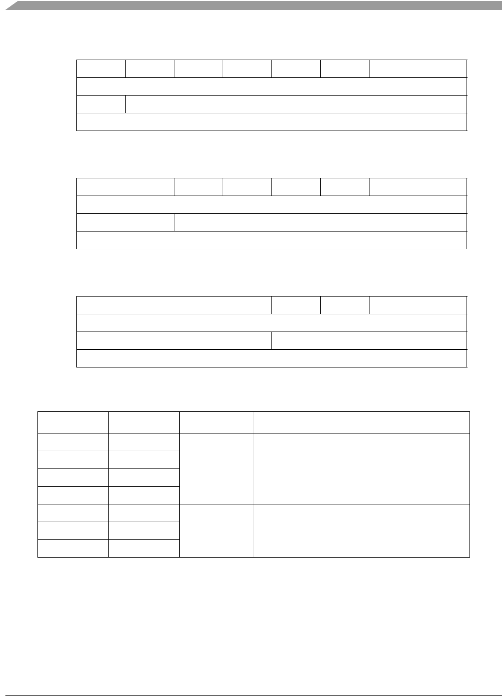
Field — DDRn6DDRn5DDRn4DDRn3DDRn2DDRn1DDRn0
Reset 0000_0000
R/W: R R/W
Address IPSBAR + 0x10_0021(DDRQS)
Figure 26-8. Port Data Direction Register (7-bit)
76543210
Field — DDRn5DDRn4DDRn3DDRn2DDRn1DDRn0
Reset 0000_0000
R/W: R R/W
Address IPSBAR + 0x10_0020 (DDRAS), 0x10_0022 (DDRSD)
Figure 26-9. Port Data Direction Registers (6-bit)
7 43210
Field — DDRn3DDRn2DDRn1DDRn0
Reset 0000_0000
R/W: R R/W
Address IPSBAR + 0x10_0023 (DDRTC), 0x10_0024 (DDRTD), 0x10_0025 (DDRUA)
Figure 26-10. Port Data Direction Registers (4-bit)
Table 26-4. DDRn (8-bit, 6-bit, and 4-bit) Field Descriptions
Register Bits Name Description
8-bit 7–0 DDRnx Port n data direction bits.
1Port n pin configured as an output
0Port n pin configured as an input
7-bit 6–0
6-bit 5–0
4-bit 3–0
7-bit 7 — Reserved, should be cleared.
6-bit 7–6
4-bit 7–4
MCF5282 and MCF5216 ColdFire Microcontroller User’s Manual, Rev. 3