
Datasheet


Chapter 2 Port Integration Module (PIM9C32) Block Description
108 MC9S12C-Family / MC9S12GC-Family Freescale Semiconductor
Rev 01.24
2.6 Interrupts
Port P and J generate a separate edge sensitive interrupt if enabled.
2.6.1 Interrupt Sources
NOTE
Vector addresses and their relative interrupt priority are determined at the
MCU level.
2.6.2 Recovery from STOP
The PIM can generate wake-up interrupts from STOP on port P and J. For other sources of external
interrupts please refer to the respective Block User Guide.
2.7 Application Information
It is not recommended to write PORTx and DDRx in a word access. When changing the register pins from
inputs to outputs, the data may have extra transitions during the write access. Initialize the port data register
before enabling the outputs.
Power consumption will increase the more the voltages on general purpose input pins deviate from the
supply voltages towards mid-range because the digital input buffers operate in the linear region.
Table 2-39. Port Reset State Summary
Port
Reset States
Data Direction Pull Mode Reduced Drive Wired-OR Mode Interrupt
T Input Hi-z Disabled n/a n/a
S Input Pull up Disabled Disabled n/a
M Input Pull up Disabled Disabled n/a
P Input Hi-z Disabled n/a Disabled
J Input Hi-z Disabled n/a Disabled
A
Refer to MEBI Block Guide for details.
B
E
BKGD pin Refer to BDM Block Guide for details.
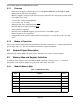
Table 2-40. Port Integration Module Interrupt Sources
Interrupt Source Interrupt Flag Local Enable Global (CCR) Mask
Port P PIFP[7:0] PIEP[7:0] I Bit
Port J PIFJ[7:6] PIEJ[7:6] I Bit