
Datasheet


MC68HC908GP32 Data Sheet, Rev. 10
Freescale Semiconductor 157
Chapter 14
System Integration Module (SIM)
14.1 Introduction
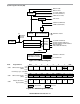
This section describes the system integration module (SIM). Together with the CPU, the SIM controls all
MCU activities. A block diagram of the SIM is shown in Figure 14-1. Table 14-1 is a summary of the SIM
input/output (I/O) registers. The SIM is a system state controller that coordinates CPU and exception
timing. The SIM is responsible for:
• Bus clock generation and control for CPU and peripherals:
– Stop/wait/reset/break entry and recovery
– Internal clock control
• Master reset control, including power-on reset (POR) and COP timeout
• Interrupt arbitration
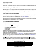
Table 14-1 shows the internal signal names used in this section.
Table 14-1. Signal Name Conventions
Signal Name Description
CGMXCLK Buffered version of OSC1 from clock generator module (CGM)
CGMVCLK PLL output
CGMOUT
PLL-based or OSC1-based clock output from CGM module
(Bus clock = CGMOUT divided by two)
IAB Internal address bus
IDB Internal data bus
PORRST Signal from the power-on reset module to the SIM
IRST Internal reset signal
R/
W Read/write signal