
Datasheet


Port E
MC68HC908GP32 Data Sheet, Rev. 10
Freescale Semiconductor 129
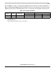
When bit DDREx is a logic 1, reading address $0008 reads the PTEx data latch. When bit DDREx is a
logic 0, reading address $0008 reads the voltage level on the pin. The data latch can always be written,
regardless of the state of its data direction bit. Table 12-6 summarizes the operation of the port E pins.
Table 12-6. Port E Pin Functions
DDRE Bit PTE Bit I/O Pin Mode
Accesses to DDRE Accesses to PTE
Read/Write Read Write
0
X
(1)
Input, Hi-Z
(2)
DDRE1–DDRE0 Pin
PTE1–PTE0
(3)
1 X Output DDRE1–DDRE0 PTE1–PTE0 PTE1–PTE0
Notes:
1. X = Don’t care
2. Hi-Z = High impedance
3. Writing affects data register, but does not affect input.