
Datasheet


Input/Output (I/O) Ports
MC68HC908GP32 Data Sheet, Rev. 10
126 Freescale Semiconductor
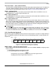
Figure 12-15 shows the port D I/O logic.
NOTE
For those devices packaged in a 40-pin dual in-line package, PTD6 and
PTD7 are not connected. DDRD6 and DDRD7 should be set to a 1 to
configure PTD6 and PTD7 as outputs.
Figure 12-15. Port D I/O Circuit
When bit DDRDx is a logic 1, reading address $0003 reads the PTDx data latch. When bit DDRDx is a
logic 0, reading address $0003 reads the voltage level on the pin. The data latch can always be written,
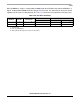
regardless of the state of its data direction bit. Table 12-5 summarizes the operation of the port D pins.
Table 12-5. Port D Pin Functions
PTDPUE Bit DDRD Bit PTD Bit I/O Pin Mode
Accesses to DDRD Accesses to PTD
Read/Write Read Write
10
X
(1)
Input, V
DD
(4)
DDRD7–DDRD0 Pin
PTD7–PTD0
(3)
00X
Input, Hi-Z
(2)
DDRD7–DDRD0 Pin
PTD7–PTD0
(3)
X 1 X Output DDRD7–DDRD0 PTD7–PTD0 PTD7–PTD0
Notes:
1. X = Don’t care
2. Hi-Z = High impedance
3. Writing affects data register, but does not affect input.
4. I/O pin pulled up to V
DD
by internal pullup device.
READ DDRD ($0007)
WRITE DDRD ($0007)
RESET
WRITE PTD ($0003)
READ PTD ($0003)
PTDx
DDRDx
PTDx
INTERNAL DATA BUS
V
DD
PTDPUEx
INTERNAL
PULLUP
DEVICE