
Datasheet

Output Compare (OC)
MC68HC711D3 Data Sheet, Rev. 2.1
Freescale Semiconductor 95
8.4.6 Timer Control 1 Register
The bits of the timer control 1 register (TCTL1) specify the action taken as a result of a successful OCx
compare.
OM2–OM5 — Output Mode Bits
OL2–OL5 — Output Level Bits
These control bit pairs are encoded to specify the action taken after a successful OCx compare. OC5
functions only if the I4/O5 bit in the PACTL register is clear. Refer to Table 8-3 for the coding.
8.4.7 Timer Interrupt Mask 1 Register
The timer interrupt mask 1 register (TMSK1) is an 8-bit register used to enable or inhibit the timer input
capture and output compare interrupts.
OC1I–OC4I — Output Compare x Interrupt Enable Bits
If the OCxI enable bit is set when the OCxF flag bit is set, a hardware interrupt sequence is requested.
I4/O5I — Input Capture 4 or Output Compare 5 Interrupt Enable Bit
When I4/O5 in PACTL is one, I4/O5I is the input capture 4 interrupt enable bit. When I4/O5 in PACTL
is 0, I4/O5I is the output compare 5 interrupt enable bit.
IC1I–IC3I — Input Capture x Interrupt Enable Bits
If the ICxI enable bit is set when the ICxF flag bit is set, a hardware interrupt sequence is requested.
NOTE
Bits in TMSK1 correspond bit for bit with flag bits in TFLG1. Ones in TMSK1
enable the corresponding interrupt sources.
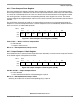
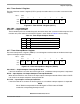
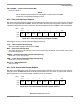
Address: $0020
Bit 7654321Bit 0
Read:
OM2OL2OM3OL3OM4OL4OM5OL5
Write:
Reset:00000000
Figure 8-11. Timer Control 1 Register (TCTL1)
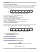
Table 8-3. Timer Output Compare Actions
OMx OLx Action Taken on Successful Compare
0 0 Timer disconnected from output pin logic
0 1 Toggle OCx output line
1 0 Clear OCx output line to 0
1 1 Set OCx output line to 1
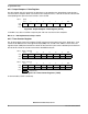
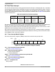
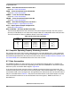
Address: $0022
Bit 7654321Bit 0
Read:
OC1I OC2I OC3I OC4I I4/O5I IC1I IC2I IC3I
Write:
Reset:00000000
Figure 8-12. Timer Interrupt Mask 1 Register (TMSK1)