
Datasheet

Programmable Timer
MC68HC711D3 Data Sheet, Rev. 2.1
94 Freescale Semiconductor
8.4.4 Output Compare 1 Data Register
Use this register with OC1 to specify the data that is to be stored on the affected pin of port A after a
successful OC1 compare. When a successful OC1 compare occurs, a data bit in OC1D is stored in the
corresponding bit of port A for each bit that is set in OC1M.
If OC1Mx is set, data in OC1Dx is output to port A bit x on successful OC1 compares.
Bits 2–0 — Not implemented; always read 0.
8.4.5 Timer Counter Register
The 16-bit read-only timer count register (TCNT) contains the prescaled value of the 16-bit timer. A full
counter read addresses the most significant byte (MSB) first. A read of this address causes the least
significant byte (LSB) to be latched into a buffer for the next CPU cycle so that a double-byte read returns
the full 16-bit state of the counter at the time of the MSB read cycle.
In normal modes, TCNT is read-only.
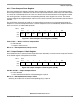
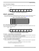
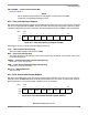
Address: $000D
Bit 7654321Bit 0
Read:
OC1D7 OC1D6 OC1D5 OC1D4 OC1D3 0 0 0
Write:
Reset:00000000
Figure 8-9. Output Compare 1 Data Register (OC1D)
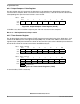
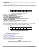
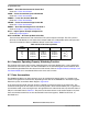
Address: $000E — TCNT High
Bit 15 14 13 12 11 10 9 Bit 8
Read: Bit 15 Bit 14 Bit 13 Bit 12 Bit 11 Bit 10 Bit 9 Bit 08
Write:
Reset:00000000
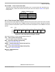
Address: $000F — TCNT Low
Bit 7654321Bit 0
Read: Bit 7 Bit 6 Bit 5 Bit 4 Bit 3 Bit 2 Bit 1 Bit 0
Write:
Reset:00000000
= Unimplemented
Figure 8-10. Timer Counter Registers (TCNT)