
Datasheet

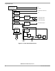

Input Capture
MC68HC711D3 Data Sheet, Rev. 2.1
Freescale Semiconductor 89
8.3.1 Timer Control 2 Register
Use the control bits of timer control 2 register (TCTL2) to program input capture functions to detect a
particular edge polarity on the corresponding timer input pin. Each of the input capture functions can be
independently configured to detect rising edges only, falling edges only, any edge (rising or falling), or to
disable the input capture function. The input capture functions operate independently of each other and
can capture the same TCNT value if the input edges are detected within the same timer count cycle.
EDGxB and EDGxA — Input Capture Edge Control
There are four pairs of these bits. Each pair is cleared to 0 by reset and must be encoded to configure
the corresponding input capture edge detector circuit. IC4 functions only if the I4/O5 bit in PACTL is
set. Refer to Table 8-2 for timer control configuration.
8.3.2 Timer Input Capture Registers
When an edge has been detected and synchronized, the 16-bit free-running counter value is transferred
into the input capture register pair as a single 16-bit parallel transfer. Timer counter value captures and
timer counter incrementing occur on opposite half-cycles of the phase two clock so that the count value
is stable whenever a capture occurs. The timer input capture (TICx) registers are not affected by reset.
Input capture values can be read from a pair of 8-bit read-only registers. A read of the high-order byte of
an input capture register pair inhibits a new capture transfer for one bus cycle. If a double-byte read
instruction, such as LDD, is used to read the captured value, coherency is assured. When a new input
capture occurs immediately after a high-order byte read, transfer is delayed for an additional cycle but the
value is not lost.
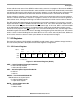
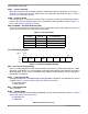
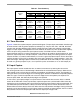
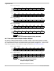
Address: $0021
Bit 7654321Bit 0
Read:
EDG4B EDG4A EDG1B EDG1A EDG2B EDG2A EDG3B EDG3A
Write:
Reset:00000000
Figure 8-3. Timer Control 2 Register (TCTL2)
Table 8-2. Timer Control Configuration
EDGxB EDGxA Configuration
0 0 Capture disabled
0 1 Capture on rising edges only
1 0 Capture on falling edges only
1 1 Capture on any edge
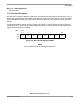
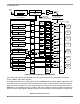
Address: $0010 — TIC1 (High)
Bit 15 14 13 12 11 10 9 Bit 8
Read: Bit 15 Bit 14 Bit 13 Bit 12 Bit 11 Bit 10 Bit 9 Bit 8
Write:
Reset: Unaffected by reset
= Unimplemented
Figure 8-4. Timer Input Capture Registers (TICx)