
Datasheet


Clock Phase and Polarity Controls
MC68HC711D3 Data Sheet, Rev. 2.1
Freescale Semiconductor 79
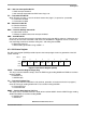
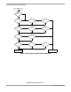
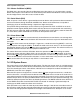
Figure 7-2. SPI Transfer Format
7.4 Clock Phase and Polarity Controls
Software can select one of four combinations of serial clock phase and polarity using two bits in the SPI
control register (SPCR). The clock polarity is specified by the CPOL control bit, which selects an active
high or active low clock, and has no significant effect on the transfer format. The clock phase (CPHA)
control bit selects one of two different transfer formats. The clock phase and polarity should be identical
for the master SPI device and the communicating slave device. In some cases, the phase and polarity
are changed between transfers to allow a master device to communicate with peripheral slaves having
different requirements.
When CPHA equals 0, the slave select (SS
) line must be negated and reasserted between each
successive serial byte. Also, if the slave writes data to the SPI data register (SPDR) while SS
is active
low, a write collision error results.
When CPHA equals 1, the SS
line can remain low between successive transfers.
7.5 SPI Signals
This subsection contains description of the four SPI signals:
• Master in/slave out (MISO)
• Master out/slave in (MOSI)
• Serial clock (SCK)
• Slave select (SS
)
7.5.1 Master In/Slave Out (MISO)
MISO is one of two unidirectional serial data signals. It is an input to a master device and an output from
a slave device. The MISO line of a slave device is placed in the high-impedance state if the slave device
is not selected.
23456781
SCK (CPOL = 1)
SCK (CPOL = 0)
SCK CYCLE #
SS
(TO SLAVE)
654321 LSBMSB
MSB654321LSB
1
2
3
5
4
SLAVE CPHA=1 TRANSFER IN PROGRESS
MASTER TRANSFER IN PROGRESS
SLAVE CPHA=0 TRANSFER IN PROGRESS
1. SS
ASSERTED
2. MASTER WRITES TO SPDR
3. FIRST SCK EDGE
4. SPIF SET
5. SS
NEGATED
SAMPLE INPUT
DATA OUT
(CPHA = 0)
SAMPLE INPUT
DATA OUT
(CPHA = 1)