
Datasheet

Input/Output (I/O) Ports
MC68HC711D3 Data Sheet, Rev. 2.1
64 Freescale Semiconductor
5.5 Port D
Port D is an 8-bit, general-purpose I/O port with a data register (PORTD) and a data direction register
(DDRD). The eight port D bits (D7–D0) can be used for general-purpose I/O, for the serial
communications interface (SCI) and serial peripheral interface (SPI) subsystems, or for bus data direction
control
5.5.1 Port D Data Register
PORTD can be read at any time and inputs return the sensed levels at the pin; whereas, outputs return
the input level of the port D pin drivers. If PORTD is written, the data is stored in an internal latch, and can
be driven only if port D is configured as general-purpose output. This port shares functions with the
on-chip SCI and SPI subsystems, while bits 6 and 7 control the direction of data flow on the bus in
expanded and special test modes.
5.5.2 Port D Data Direction Register
DDD7–DDD0 — Data Direction for Port D
When port D is a general-purpose I/O port, the DDRD register controls the direction of the I/O pins as
follows:
0 = Configures the corresponding port D pin for input only
1 = Configures the corresponding port D pin for output
In expanded and test modes, bits 6 and 7 are dedicated AS and R/W
.
When port D is functioning with the SPI system enabled, bit 5 is dedicated as the slave select (SS
)
input. In SPI slave mode, DDD5 has no meaning or effect. In SPI master mode, DDD5 affects port D
bit 5 as follows:
0 = Port D bit 5 is an error-detect input to the SPI.
1 = Port D bit 5 is configured as a general-purpose output line.
If the SPI is enabled and expects port D bits 2, 3, and 4 (MISO, MOSI, and SCK) to be inputs, then
they are inputs, regardless of the state of DDRD bits 2, 3, and 4. If the SPI expects port D bits 2, 3,
and 4 to be outputs, they are outputs only if DDRD bits 2, 3, and 4 are set.
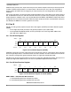
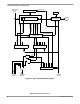
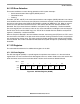
Address: $0008
Bit 7654321Bit 0
Read:
PD7 PD6 PD5 PD4 PD3 PD2 PD1 PD0
Write:
Reset:00000000
Figure 5-7. Port D Data Register (PORTD)
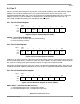
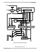
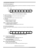
Address: $0009
Bit 7654321Bit 0
Read:
DDD7 DDD6 DDD5 DDD4 DDD3 DDD2 DDD1 DDD0
Write:
Reset:00000000
Figure 5-8. Data Direction Register for Port D (DDRD)