
Datasheet


MC68L11D0 Electrical Characteristics
MC68HC711D3 Data Sheet, Rev. 2.1
Freescale Semiconductor 133
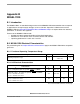
B.2.3 Control Timing
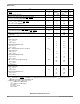
B.2.4 Peripheral Port Timing
Characteristic
(1)
1. V
DD
= 3.0 Vdc to 5.5 Vdc, V
SS
= 0 Vdc, T
A
= T
L
to T
H
. All timing is shown with respect to 20% V
DD
and 70% V
DD
, unless
otherwise noted.
Symbol
1.0 MHz 2.0 MHz
Unit
Min Max Min Max
Frequency of operation
f
O
dc 1.0 dc 2.0 MHz
E-clock period
t
cyc
1000 — 500 — ns
Crystal frequency
f
XTAL
— 4.0 — 8.0 MHz
External oscillator frequency
4 f
O
dc 4.0 dc 8.0 MHz
Processor control setup time
t
PCSU
= 1/4 t
cyc
+ 50 ns
t
PCSU
325 — 200 — ns
Reset input pulse width
(2)
To guarantee external reset vector
Minimum input time can be preempted by internal reset
2. Reset is recognized during the first clock cycle it is held low. Internal circuitry then drives the pin low for four clock cycles,
releases the pin, and samples the pin level two cycles later to determine the source of the interrupt. Refer to Chapter 4
Resets, Interrupts, and Low-Power Modes for further details.
PW
RSTL
8
1
—
—
8
1
—
—
t
cyc
Interrupt pulse width, PW
IRQ
= t
cyc
+ 20 ns
IRQ
edge-sensitive mode
PW
IRQ
1020 — 520 — ns
Wait recovery startup time
t
WRS
—4—4
t
cyc
Timer pulse width PW
TIM
= t
cyc
+ 20 ns
Input capture pulse accumulator input
PW
TIM
1020 — 520 — ns
Characteristic
(1)
1. V
DD
= 3.0 Vd to 5.5 Vdc, V
SS
= 0 Vdc, T
A
= T
L
to T
H
. All timing is shown with respect to 20% V
DD
and 70% V
DD
, unless
otherwise noted.
Symbol
1.0 MHz 2.0 MHz
Unit
Min Max Min Max
Frequency of operation (E-clock frequency)
f
O
dc 1.0 dc 2.0 MHz
E-clock period
t
cyc
1000 — 500 — ns
Peripheral data setup time
(2)
MCU read of ports A, B, C, and D
2. Port C and D timing is valid for active drive (CWOM and DWOM bits not set in PIOC and SPCR registers respectively).
t
PDSU
100 — 100 — ns
Peripheral data hold time
(2)
MCU read of ports A, B, C, and D
t
PDH
50 — 50 — ns
Delay time, peripheral data write
MCU write to port A
MCU writes to ports B, C, and D
t
PWD
= 1/4 t
cyc
+ 150 ns
t
PWD
—
—
200
350
—
—
200
225
ns