
Datasheet
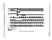

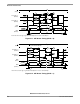


Expansion Bus Timing
MC68HC711D3 Data Sheet, Rev. 2.1
Freescale Semiconductor 115
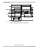
9.8 Expansion Bus Timing
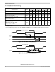
Num
Characteristic
(1)
1. V
DD
= 5.0 Vdc ± 10%, V
SS
= 0 Vdc, T
A
= T
L
to T
H
. All timing is shown with respect to 20% V
DD
and 70% V
DD
, unless
otherwise noted.
Symbol
1.0 MHz 2.0 MHz 3.0 MHz
Unit
Min Max Min Max Min Max
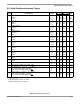
Frequency of operation (E-clock frequency)
f
O
dc 1.0 dc 2.0 dc 3.0 MHz
1 Cycle time
t
cyc
1000 — 500 — 333 — ns
2
Pulse width, E low, PW
EL
= 1/2 t
cyc
— 23 ns PW
EL
477 — 227 — 146 — ns
3
Pulse width, E high, PW
EH
= 1/2 t
cyc
– 28 ns PW
EH
472 — 222 — 141 — ns
4A E and AS rise time
t
r
—20—20—20ns
4B E and AS fall time
t
f
—20—20—15ns
9
Address hold time
(2)a
, t
AH
= 1/8 t
cyc
– 29.5 ns
2. Input clocks with duty cycles other than 50% affect bus performance. Timing parameters affected by input clock duty cycle
are identified by (a) and (b). To recalculate the approximate bus timing values, substitute the following expressions in place
of 1/8 t
CYC
in the above formulas, where applicable:
(a) (1-dc) × 1/4 t
CYC
(b) dc × 1/4 t
CYC
Where:
DC is the decimal value of duty cycle percentage (high time).
t
AH
95.5 — 33 — 26 — ns
12
Non-muxed address valid time to E rise
t
AV
= PW
EL
– (t
ASD
+ 80 ns)
(2)a
t
AV
281.5 — 94 — 54 — ns
17 Read data setup time
t
DSR
30 — 30 — 30 — ns
18
Read data hold time (max = t
MAD
)t
DHR
0 145.5 0 83 0 51 ns
19
Write data delay time, t
DDW
= 1/8 t
cyc
+ 65.5 ns
(2)a
t
DDW
— 190.5 — 128 — 71 ns
21
Write data hold time, t
DHW
= 1/8 t
cyc
– 29.5 ns
(2)a
t
DHW
95.5 — 33 — 26 — ns
22
Muxed address valid time to E rise
t
AVM
= PW
EL
– (t
ASD
+ 90 ns)
(2)a
t
AVM
271.5 — 84 — 54 — ns
24
Muxed address valid time to AS fall
t
ASL
= PW
ASH
– 70 ns
t
ASL
151 — 26 — 13 — ns
25
Muxed address hold time, t
AHL
= 1/8 t
cyc
– 29.5 ns
(2)b
t
AHL
95.5 — 33 — 31 — ns
26
Delay time, E to AS rise, t
ASD
= 1/8 t
cyc
– 9.5 ns
(2)a
t
ASD
115.5 — 53 — 31 — ns
27
Pulse width, AS high, PW
ASH
= 1/4 t
cyc
– 29 ns PW
ASH
221 — 96 — 63 — ns
28
Delay time, AS to E rise, t
ASED
= 1/8 t
cyc
– 9.5 ns
(2)b
t
ASED
115.5 — 53 — 31 — ns
29
MPU address access time
(2)a
t
ACCA
= t
cyc
– (PW
EL
– t
AVM
) – t
DSR
– t
f
t
ACCA
744.5 — 307 — 196 — ns
35
MPU access time , t
ACCE
= PW
EH
– t
DSR
t
ACCE
— 442 — 192 — 111 ns
36
Muxed address delay (previous cycle MPU read)
t
MAD
= t
ASD
+ 30 ns
(2)a(3)
3. Formula only for dc to 2 MHz.
t
MAD
145.5 — 83 — 51 — ns