
Datasheet


Electrical Characteristics
MC68HC711D3 Data Sheet, Rev. 2.1
106 Freescale Semiconductor
9.3 Functional Operating Temperature Range
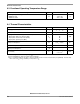
9.4 Thermal Characteristics
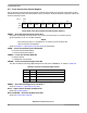
Rating Symbol Value Unit
Operating temperature range
MC68HC711D3
MC68HC711D3V
T
A
T
L
to T
H
–40 to +85
–40 to +105
°C
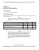
Characteristic Symbol Value Unit
Average junction temperature
T
J
T
A
+ (P
D
× Θ
JA
)
°C
Ambient temperature
T
A
User-determined °C
Package thermal resistance (junction-to-ambient)
40-pin plastic dual in-line package (DIP)
44-pin plastic leaded chip carrier (PLCC)
44-pin plastic quad flat pack (QFP)
Θ
JA
50
50
85
°C/W
Total power dissipation
(1)
1. This is an approximate value, neglecting P
I/O
.
P
D
P
INT
+ P
I/O
K / T
J
+ 273°C
W
Device internal power dissipation
P
INT
I
DD
× V
DD
W
I/O pin power dissipation
(2)
2. For most applications, P
I/O
≤ P
INT
and can be neglected.
P
I/O
User-determined W
A constant
(3)
3. K is a constant pertaining to the device. Solve for K with a known T
A
and a measured P
D
(at equilibrium). Use this value
of K to solve for P
D
and T
J
, iteratively, for any value of T
A
.
K
P
D
× (T
A
+ 273°C)
+ Θ
JA
× P
D
2
W/°C