
Datasheet


DRAFT
DRAFT DRAFT DR
DRAFT DRAFT DRAFT
D
RAF
DRAFT DRAFT DRA
F
T D
RAFT DR
AFT D
DRA
F
T DRAFT DRAFT
D
RAFT
DRAFT
D
RAFT
DRA
LPC82x All information provided in this document is subject to legal disclaimers. © NXP Semiconductors N.V. 2014. All rights reserved.
Product data sheet Rev. 0.11 — 26 August 2014 67 of 81
NXP Semiconductors
LPC82x
32-bit ARM Cortex-M0+ microcontroller
14. Application information
14.1 XTAL input
The input voltage to the on-chip oscillators is limited to 1.8 V. If the oscillator is driven by a
clock in slave mode, it is recommended that the input be coupled through a capacitor with
C
i
= 100 pF. To limit the input voltage to the specified range, choose an additional
capacitor to ground C
g
which attenuates the input voltage by a factor C
i
/(C
i
+ C
g
). In slave
mode, a minimum of 200 mV(RMS) is needed.
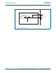
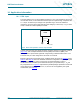
In slave mode the input clock signal should be coupled by means of a capacitor of 100 pF
(Figure 40
), with an amplitude between 200 mV (RMS) and 1000 mV (RMS). This
corresponds to a square wave signal with a signal swing of between 280 mV and 1.4 V.
The XTALOUT pin in this configuration can be left unconnected.
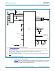
External components and models used in oscillation mode are shown in Figure 41
and in
Tab le 2 7
and Tab le 28. Since the feedback resistance is integrated on chip, only a crystal
and the capacitances C
X1
and C
X2
need to be connected externally in case of
fundamental mode oscillation (the fundamental frequency is represented by L, C
L
and
R
S
). Capacitance C
P
in Figure 41 represents the parallel package capacitance and should
not be larger than 7 pF. Parameters F
OSC
, C
L
, R
S
and C
P
are supplied by the crystal
manufacturer (see Tab le 2 7
).
Fig 40. Slave mode operation of the on-chip oscillator
/3&
;7$/,1
&
L
S)
&
J
DDD