
Datasheet


LPC408X_7X All information provided in this document is subject to legal disclaimers. © NXP Semiconductors N.V. 2014. All rights reserved.
Product data sheet Rev. 3.1 — 1 September 2014 101 of 138
NXP Semiconductors
LPC408x/7x
32-bit ARM Cortex-M4 microcontroller
11.8 I
2
S-bus interface
[1] CCLK = 100 MHz; peripheral clock to the I
2
S-bus interface PCLK = CCLK / 4. I
2
S clock cycle time T
cy(clk)
=
1600 ns, corresponds to the SCK signal in the I
2
S-bus specification.
Table 24. Dynamic characteristics: I
2
S-bus interface pins
C
L
=10pF, T
amb
=
40
C to 85
C, V
DD(3V3)
= 3.0 V to 3.6 V. Values guaranteed by design.
Symbol Parameter Conditions Min Max Unit
common to input and output
t
r
rise time
[1]
-6.7ns
t
f
fall time
[1]
-8.0ns
t
WH
pulse width HIGH on pins I2S_TX_SCK and
I2S_RX_SCK
[1]
25 - -
t
WL
pulse width LOW on pins I2S_TX_SCK and
I2S_RX_SCK
[1]
-25ns
output
t
v(Q)
data output valid time on pin I2S_TX_SDA;
[1]
-6ns
input
t
su(D)
data input set-up time on pin I2S_RX_SDA
[1]
5- ns
t
h(D)
data input hold time on pin I2S_RX_SDA
[1]
2- ns
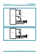
Fig 27. I
2
S-bus timing (transmit)
002aag202
I2S_TX_SCK
I2S_TX_SDA
I2S_TX_WS
T
cy(clk)
t
f
t
r
t
WH
t
WL
t
v(Q)
t
v(Q)