
Microcontrollers User manual

UM10237_2 © NXP B.V. 2008. All rights reserved.
User manual Rev. 02 — 19 December 2008 721 of 792
NXP Semiconductors
UM10237
Chapter 32: LPC24XX General Purpose DMA (GPDMA) controller
[1] Reset Value reflects the data stored in used bits only. It does not include reserved bits content.
[2] Bit [17] is read-only.
6.1 General GPDMA registers
This section describes the registers of the GPDMA.
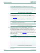
6.1.1 Interrupt Status Register (DMACIntStatus - 0xFFE0 4000)
The DMACIntStatus Register is read-only and shows the status of the interrupts after
masking. A HIGH bit indicates that a specific DMA channel interrupt request is active. The
request can be generated from either the error or terminal count interrupt requests.
Table 32–654
shows the bit assignments of the DMACIntStatus Register.
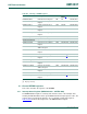
DMACEnbldChns Enabled Channel Register RO 0x0 0xFFE0 401C
DMACSoftBReq Software Burst Request
Register
R/W 0x0000 0xFFE0 4020
DMACSoftSReq Software Single Request
Register
R/W 0x0000 0xFFE0 4024
DMACSoftLBReq Software Last Burst Request
Register
R/W 0x0000 0xFFE0 4028
DMACSoftLSReq Software Last Single Request
Register
R/W 0x0000 0xFFE0 402C
DMACConfiguration Configuration Register R/W 0x0000 0000 0xFFE0 4030
DMACSync Synchronization Register R/W 0x0000 0xFFE0 4034
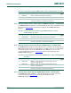
Channel 0 Registers
DMACC0SrcAddr Channel 0 Source Address
Register
R/W 0x0000 0000 0xFFE0 4100
DMACC0DestAddr Channel 0 Destination
Address Register
R/W 0x0000 0000 0xFFE0 4104
DMACC0LLI Channel 0 Linked List Item
Register
R/W 0x0000 0000 0xFFE0 4108
DMACC0Control Channel 0 Control Register R/W 0x0000 0000 0xFFE0 410C
DMACC0Configuration Channel 0 Configuration
Register
R/W 0x00000
[2]
0xFFE0 4110
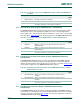
Channel 1 Registers
DMACC1SrcAddr Channel 1 Source Address
Register
R/W 0x0000 0000 0xFFE0 4120
DMACC1DestAddr Channel 1 Destination
Address Register
R/W 0x0000 0000 0xFFE0 4124
DMACC1LLI Channel 1 Linked List Item
Register
R/W 0x0000 0000 0xFFE0 4128
DMACC1Control Channel 1 Control Register R/W 0x0000 0000 0xFFE0 412C
DMACC1Configuration Channel 1 Configuration
Register
R/W 0x00000
[2]
0xFFE0 4130
Table 653. Summary of GPDMA registers
Name Description Access Reset
Value
[1]
Address