
Microcontrollers User manual


UM10237_2 © NXP B.V. 2008. All rights reserved.
User manual Rev. 02 — 19 December 2008 714 of 792
NXP Semiconductors
UM10237
Chapter 32: LPC24XX General Purpose DMA (GPDMA) controller
4.2.4 Channel Logic and Channel Register Bank
The channel logic and channel register bank contains registers and logic required for each
DMA channel.
4.2.5 Interrupt Request
The interrupt request generates interrupts to the ARM processor.
4.2.6 AHB Master Interface
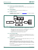
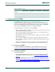
The GPDMA contains a full AHB master. See Figure 32–145 for an example showing the
GPDMA connected into a system.
The AHB master is capable of dealing with all types of AHB transactions, including:
• Split, retry, and error responses from slaves. If a peripheral performs a split or retry,
the GPDMA stalls and waits until the transaction can complete.
• Locked transfers for source and destination of each stream.
• Setting of protection bits for transfers on each stream.
4.2.7 Bus and transfer widths
The physical width of the AHB bus is 32 bits. Source and destination transfers can be of
differing widths, and can be the same width or narrower than the physical bus width. The
GPDMA packs or unpacks data as appropriate.
4.2.8 Endian behavior
The GPDMA can cope with both little-endian and big-endian addressing. You can set the
endianness of each AHB master individually.
Internally the GPDMA treats all data as a stream of bytes instead of 16 bit or 32 bit
quantities. This means that when performing mixed-endian activity, where the endianness
of the source and destination are different, byte swapping of the data within the 32 bit data
bus is observed.
Note: If you do not require byte swapping then avoid using different endianness between
the source and destination addresses.
Fig 145. Example of GPDMA in a system
GPDMA
EXTERNAL
MEMORY
AHB
PERIPHERAL
EXTERNAL
MEMORY
CONTROLLER
AHB
MASTER
AHB
SLAVE
ARM
AHB
BRIDGE
APB
BRIDGE
UART
TIMER
GPIO
INTERNAL
SRAM