
Microcontrollers User manual


UM10237_2 © NXP B.V. 2008. All rights reserved.
User manual Rev. 02 — 19 December 2008 674 of 792
1. Basic configuration
The DAC is configured using the following registers:
1. Power: The DAC is always on.
2. Clock: In the PCLK_SEL0 register (Table 4–56
), select PCLK_DAC.
3. Pins: Select the DAC pin and pin mode in registers PINSEL1 and PINMODE1 (see
Section 9–5
).
2. Features
• 10 bit digital to analog converter
• Resistor string architecture
• Buffered output
• Power down mode
• Selectable speed vs. power
3. Pin description
Table 29–599 gives a brief summary of each of DAC related pins.
Remark: When the DAC is not used, the V
DDA
and VREF pins must be connected to the
power supply, and pin V
SSA
must be grounded. These pins should not be left floating.
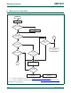
4. Register description (DACR - 0xE006 C000)
This read/write register includes the digital value to be converted to analog, and a bit that
trades off performance vs. power. Bits 5:0 are reserved for future, higher-resolution D/A
converters.
UM10237
Chapter 29: LPC24XX Digital-to Analog Converter (DAC)
Rev. 02 — 19 December 2008 User manual
Table 599. D/A Pin Description
Pin Type Description
AOUT Output Analog Output. After the selected settling time after the DACR is
written with a new value, the voltage on this pin (with respect to
V
SSA
) is VALUE/1024 × VREF.
VREF Reference
Voltage Reference. This pin provides a voltage reference level for
the D/A converter.
V
DDA
, V
SSA
Power Analog Power and Ground. These should be nominally the same
voltages as V
DD(3V3)
and V
SS
, but should be isolated to minimize
noise and error.