
Microcontrollers User manual


UM10237_2 © NXP B.V. 2008. All rights reserved.
User manual Rev. 02 — 19 December 2008 64 of 792
NXP Semiconductors
UM10237
Chapter 4: LPC24XX Clocking and power control
Some peripherals, particularly those that include analog functions, may consume power
that is not clock dependent. These peripherals may contain a separate disable control that
turns off additional circuitry to reduce power. Information on peripheral specific power
saving features may be found in the chapter describing that peripheral.
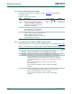
Each bit in PCONP controls one peripheral as shown in Table 4–63
. The bit numbers
correspond to the related peripheral number as shown in the APB peripheral map Table
2–17 “APB peripherals and base addresses” in the "LPC2400 Memory Addressing"
chapter.
If a peripheral control bit is 1, that peripheral is enabled. If a peripheral bit is 0, that
peripheral’s clock is disabled (gated off) to conserve power. For example if bit 19 is 1, the
I
2
C1 interface is enabled. If bit 19 is 0, the I
2
C1 interface is disabled.
Important: valid read from a peripheral register and valid write to a peripheral
register is possible only if that peripheral is enabled in the PCONP register!
Table 63. Power Control for Peripherals register (PCONP - address 0xE01F C0C4) bit
description
Bit Symbol Description Reset
value
0 - Unused, always 0 0
1 PCTIM0 Timer/Counter 0 power/clock control bit. 1
2 PCTIM1 Timer/Counter 1 power/clock control bit. 1
3 PCUART0 UART0 power/clock control bit. 1
4 PCUART1 UART1 power/clock control bit. 1
5 PCPWM0 PWM0 power/clock control bit. 1
6 PCPWM1 PWM1 power/clock control bit. 1
7PCI2C0The I
2
C0 interface power/clock control bit. 1
8 PCSPI The SPI interface power/clock control bit. 1
9 PCRTC The RTC power/clock control bit. 1
10 PCSSP1 The SSP1 interface power/clock control bit. 1
11 PCEMC External Memory Controller 1
12 PCAD A/D converter (ADC) power/clock control bit.
Note: Clear the PDN bit in the AD0CR before clearing this bit, and set
this bit before setting PDN.
0
13 PCCAN1 CAN Controller 1 power/clock control bit. 0
14 PCCAN2 CAN Controller 2 power/clock control bit. 0
18:15 - Reserved, user software should not write ones to reserved bits. The
value read from a reserved bit is not defined.
19 PCI2C1 The I
2
C1 interface power/clock control bit. 1
20 PCLCD
[1]
LCD controller power control bit. 0
21 PCSSP0 The SSP0 interface power/clock control bit. 1
22 PCTIM2 Timer 2 power/clock control bit. 0
23 PCTIM3 Timer 3 power/clock control bit. 0
24 PCUART2 UART 2 power/clock control bit. 0
25 PCUART3 UART 3 power/clock control bit. 0
26 PCI2C2 I
2
S interface 2 power/clock control bit. 1