
Microcontrollers User manual


UM10237_2 © NXP B.V. 2008. All rights reserved.
User manual Rev. 02 — 19 December 2008 613 of 792
NXP Semiconductors
UM10237
Chapter 23: LPC24XX I
2
S interface
5. Register description
Table 23–531 shows the registers associated with the I
2
S interface and a summary of
their functions. Following the table are details for each register.
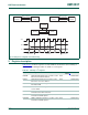
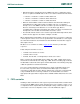
Fig 127. Simple I
2
S configurations and bus timing
TRANSMITTER
(MASTER)
CONTROLLER
(MASTER)
TRANSMITTER
(SLAVE)
RECEIVER
(MASTER)
SCK: serial clock
WS: word select
SD: serial data
TRANSMITTER
(SLAVE)
RECEIVER
(SLAVE)
SCK
WS
SD
SCK
WS
SD
MSB LSB MSB
word n
left channel
word n+1
right channel
word n-1
right channel
RECEIVER
(SLAVE)
SCK: serial clock
WS: word select
SD: serial data
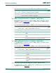
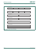
Table 531. Summary of I
2
S registers
Name Description Access Reset
Value
[1]
Address
I2SDAO Digital Audio Output Register. Contains control
bits for the I
2
S transmit channel.
R/W 0xE008 8000
I2SDAI Digital Audio Input Register. Contains control
bits for the I
2
S receive channel.
R/W 0xE008 8004
I2STXFIFO Transmit FIFO. Access register for the 8
× 32 bit
transmitter FIFO.
WO 0xE008 8008
I2SRXFIFO Receive FIFO. Access register for the 8
× 32 bit
receiver FIFO.
RO 0xE008 800C
I2SSTATE Status Feedback Register. Contains status
information about the I
2
S interface.
RO 0xE008 8010
I2SDMA1 DMA Configuration Register 1. Contains control
information for DMA request 1.
R/W 0xE008 8014
I2SDMA2 DMA Configuration Register 2. Contains control
information for DMA request 2.
R/W 0xE008 8018